AWL9224RS28Q1 データシートの表示(PDF) - ANADIGICS
部品番号
コンポーネント説明
メーカー
AWL9224RS28Q1 Datasheet PDF : 12 Pages
| |||
AWL9224
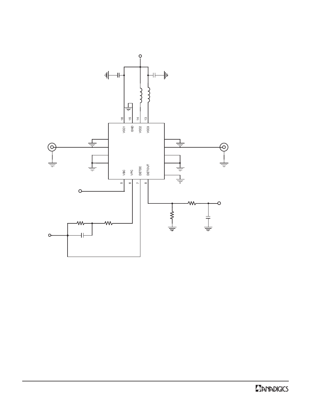
APPLICATION INFORMATION
C1
0.1uF
+ / -10%
VCC
C2
0.1uF
+ / -10%
L2
5.6nH
L1
5.6nH
U1
1
GND
12
GND
2
11
J3
RF IN
RF OUT
J4
3 GND AWL 9224
10
GND
4
GND
9
GND
25
GND
VCC
R1
174
+/-1%
R6
1K
+/-5%
R5
1K
+/-5%
VDET
C7
10pF
+/-0.5pF
VPC
C6
0.47uF
+ / -10%
R2
910
+/-5%
**NOTES**
1. RF traces should be 18 mils wide with 20 mils of clearance
2. DC traces should be 8 mils wide with 8 mils of clearance
3. Trace widths and clearances apply to application
circuit on 10 mil FR4
4. DNP = Do Not Place
5. Pin 25 is the metallized Ground slug on the LPCC package.
6. Pins 1, 3, 10, and 12 should be tied directly to PCB ground pattern
under Pin 25, and should form a coplanar waveguide for the RF In and
RF Out.
Figure 19: Application Circuit
10
PRELIMINARY DATA SHEET - Rev 1.3
04/2005
Share Link: 