M34C00 гғҮгғјгӮҝгӮ·гғјгғҲгҒ®иЎЁзӨәпјҲPDFпјү - STMicroelectronics
йғЁе“Ғз•ӘеҸ·
гӮігғігғқгғјгғҚгғігғҲиӘ¬жҳҺ
гғЎгғјгӮ«гғј
M34C00 Datasheet PDF : 15 Pages
| |||
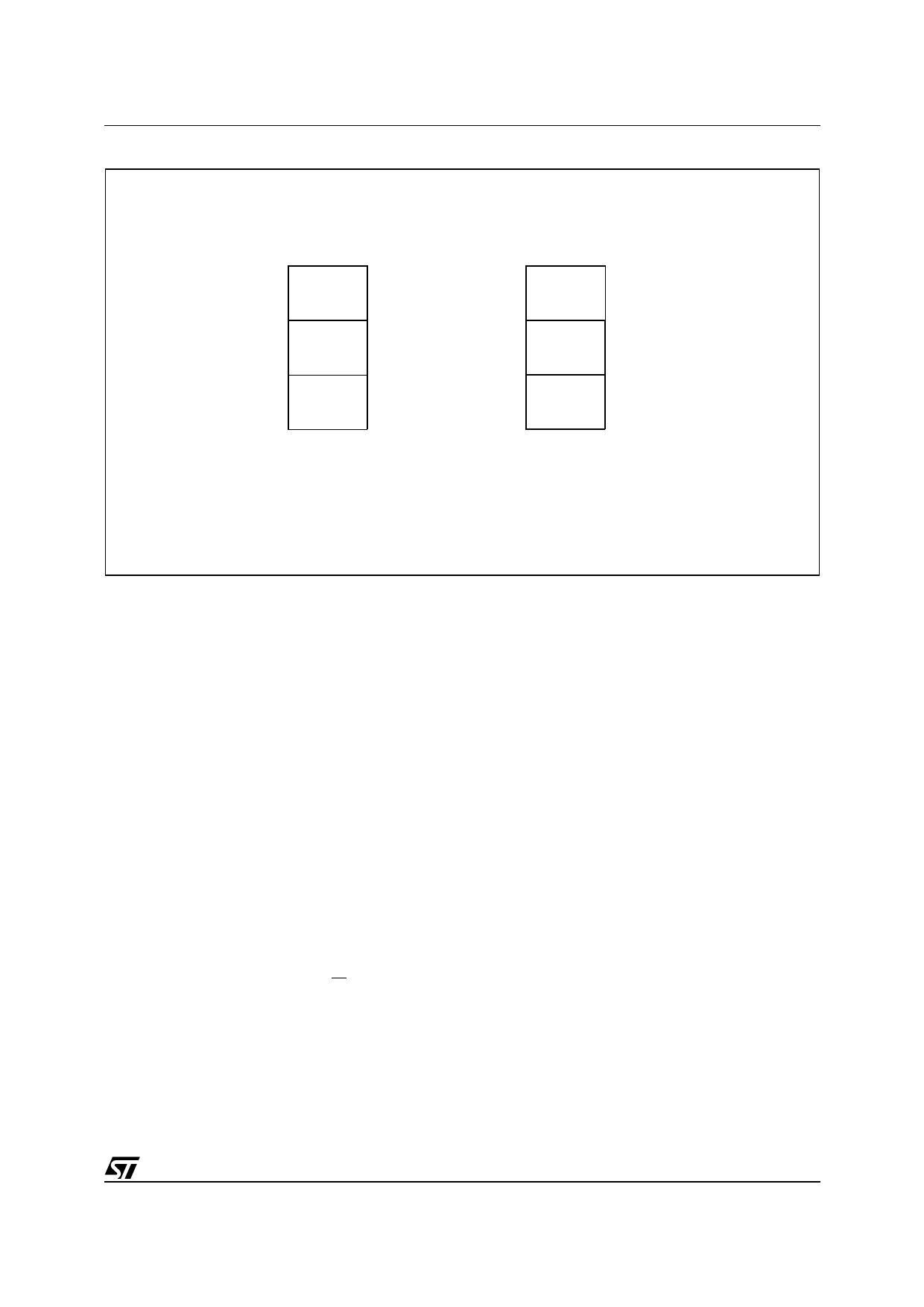
Figure 5. Memory Partitioning
M34C00
Array 2
Array 1
Array 0
2Fh
EPROM
Array
20h
1Fh
Standard
Array
10h
0Fh
Standard
Array
00h
Default EEPROM memory area
state before write access
to the Protection Register
Array 2
Array 1
Array 0
2Fh
EPROM
Array
20h
1Fh
Standard
Array
10h
0Fh
Write
Protected
Array
00h
State of the EEPROM memory
area after write access
to the Protection Register
AI03396
address the Invalid array, and immediately
deselects itself.
The Write-protectable array consists of 16 bytes of
EEPROM, which can be used as normal EEPROM
until this array is set in its Write-protected mode.
Once Write-protected, this array becomes
functionally equivalent to a Read-Only Memory
(ROM), and cannot be modified further. The
procedure to set this array in its Write-protected
mode is described later.
Array-2 also consists of 16 bytes of EEPROM, but
configured to give the functional equivalence of
non-erasable memory. That is, it is initialized to
contain all 1s (FFh), with the user able to reset any
1 to a 0, but unable to set any 0 to a 1. One
application envisaged for this array is as a non-
resettable 128-token array.
WRITE AND READ OPERATIONS
Write Operations
Following a Start condition the bus master sends
a Device Select code with the RW bit reset to 0.
The device acknowledges this, as shown in Figure
6, and waits for an address byte. The device
responds to the address byte with an acknowledge
bit, and then waits for the data byte.
Byte Write
After the Device Select code and the address byte,
the bus master sends one data byte. If the
addressed location is in the Write-protected area,
the device replies with NoAck, and the location is
not modified. If, instead, the addressed location is
not in a Write-protected area, the device replies
with Ack. The bus master terminates the transfer
by generating a Stop condition, as shown in Figure
6.
During the internal Write cycle, Serial Data (SDA)
is disabled internally, and the device does not
respond to any requests.
Minimizing System Delays by Polling On ACK
During the internal Write cycle, the device
disconnects itself from the bus, and copies the
data from its internal latches to the memory cells.
The maximum Write time (tw) is shown in Table 6,
but the typical time is shorter. To make use of this,
an Ack polling sequence can be used by the bus
master.
The sequence, as shown in Figure 7, is:
вҖ“ Initial condition: a Write cycle is in progress.
вҖ“ Step 1: the bus master issues a Start condition
followed by a Device Select code (the first byte
of the new instruction).
вҖ“ Step 2: if the device is busy with the internal
Write cycle, no Ack will be returned and the bus
master goes back to Step 1. If the device has
terminated the internal Write cycle, it responds
with an Ack, indicating that the device is ready
to receive the second part of the next instruction
(the first byte of this instruction having been sent
during Step 1).
5/15
Share Link: 