W91560 データシートの表示(PDF) - Winbond
部品番号
コンポーネント説明
メーカー
W91560 Datasheet PDF : 18 Pages
| |||
W91560N SERIES
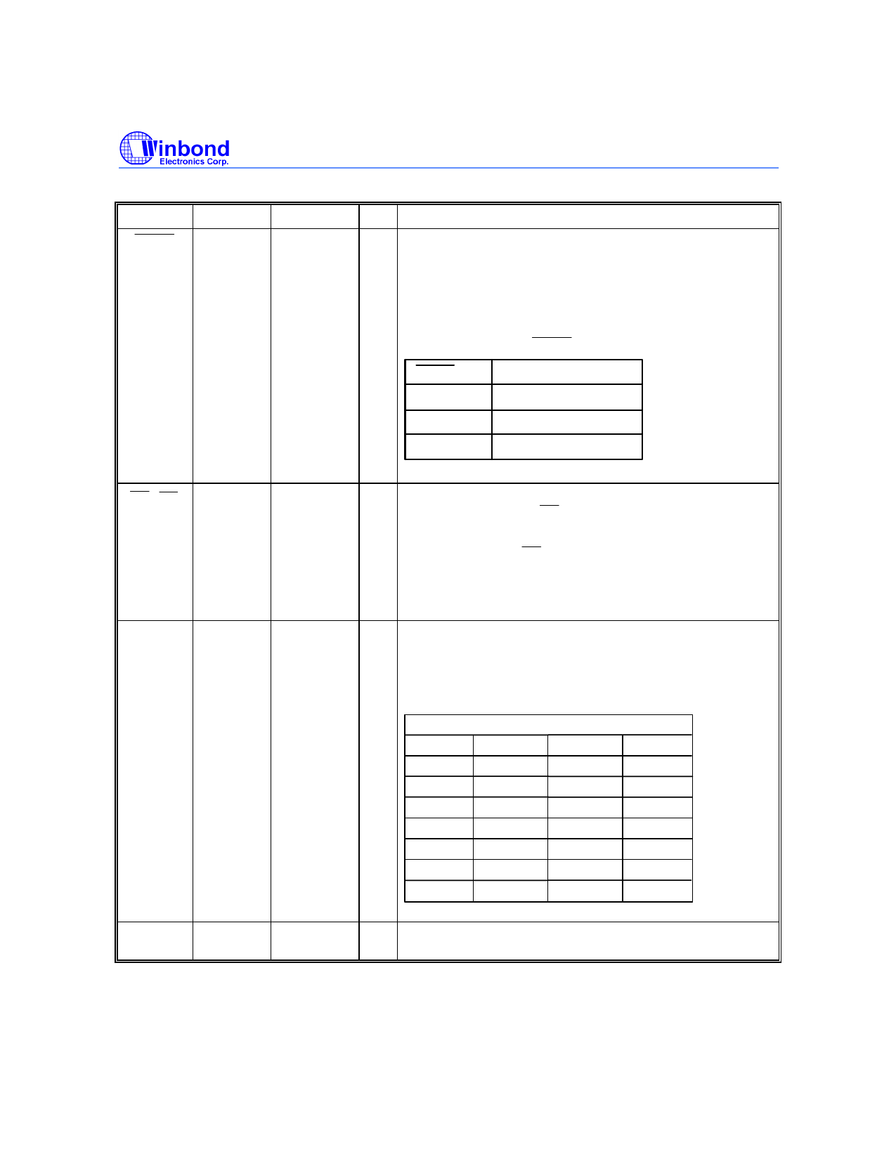
Pin Description, continued
SYMBOL 18-PIN
20-PIN I/O
FUNCTION
LOCK
5
(only for
W91561LN)
5
(only for
W91561ALN)
I The function of this terminal is to prevent "0" dialing and
"9" dialing under PABX system long distance call
control. When the first key input after reset is 0 or 9, all
key inputs, including the 0 or 9 key, become invalid and
the chip generates no output. The telephone is
reinitialized by a reset.
The function of the LOCK pin is shown below:
LOCK PIN
FUNCTION
VDD
"0", "9" dialing inhibited
Floating
Normal dialing mode
VSS
"0" dialing inhibited
DP / C5
11
DTMF
12
VDD, VSS 14, 6
13
14
16, 6
O N-channel open drain dialing pulse output.
Flash key will cause DP to be active in either tone mode
or pulse mode.
In lock mode, the DP remains low for 300 mS during off-
hook delay time.
The timing diagram for pulse mode is shown in Figure 1
(a, b, c, d).
O During pulse dialing, this pin remains in low state
regardless of keypad input. In the tone mode, it will
output a dual or single tone.
A detailed timing diagram for tone mode is shown in
Figure 2(a, b, c, d).
OUTPUT FREQUENCY
Specified
R1
697
Actual
699
Error %
+0.28
R2
770
766
-0.52
R3
852
848
-0.47
R4
941
948
+0.74
C1
1209
1216
+0.57
C2
1336
1332
-0.30
C3
1477
1472
-0.34
I Power input pins for the dialer chip. VDD is the main
power and VSS is the ground.
-4-
Share Link: 