LB1882V データシートの表示(PDF) - SANYO -> Panasonic
部品番号
コンポーネント説明
メーカー
LB1882V Datasheet PDF : 9 Pages
| |||
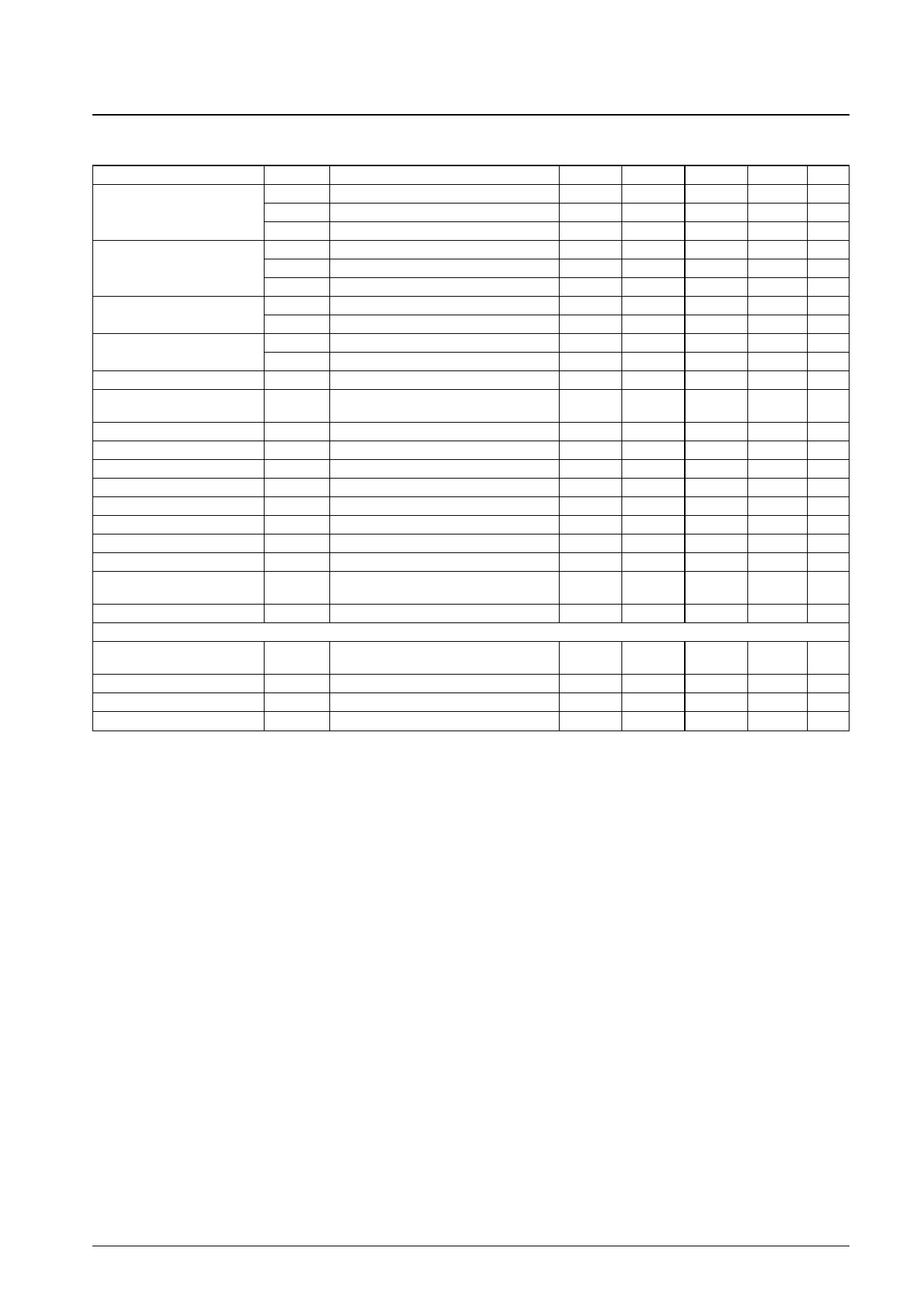
LB1882V
Electrical Characteristics at Ta = 25°C, VCC1 = 2.5 V, VCC2 = 4.5 V, VS = 1 V
Parameter
Symbol
Conditions
Current drain
Output quiescent current
Output saturation voltage
upper side
Output residual voltage
lower side
Hall amplifier input offset voltage
Hall amplifier common-mode
input voltage range
ICC1
ICC2
IS
ICC 1OQ
ICC 2OQ
ISOQ
VOU (sat)1
VOU (sat)2
VOD (sat)1
VOD (sat)2
VHoffset
IS – IL
VSTBY = 0 V
VSTBY = 0 V
VSTBY = 0 V
VRF = 40 mV, RL = 100 Ω (Y)
VRF = 100 mV, RL = 100 Ω (Y)
VRF = 40 mV, RL = 100 Ω (Y)
VRF = 100 mV, RL = 100 Ω (Y)
VHCOM
Standby pin high level voltage
Standby pin low level voltage
Standby pin input current
Standby pin leakage current
FRC pin high level voltage
FRC pin low level voltage
FRC pin input current
FRC pin leakage current
Thermal shutdown operating
temperature
VSTBYH
VSTBYL
ILSTBY
ILSTBY
VFRCH
VFRCL
IIFRC
ILFRC
TTSD
VSTBY = 4.5 V
VSTBY = 0 V
VFRC = 4.5 V
VFRC = 0 V
Thermal shutdown hysteresis
[FG Amplifier]
∆TTSD
Common-mode input
voltage range
VICR
Input offset voltage
Output saturation voltage
Output current (sink)
VIO
VSINK
ISINK
RL = 10 kΩ
Note: * Items marked with an asterisk are design target values and are not tested.
min
typ
max
Unit
Note
5
8
mA
2
mA
1
mA
10
µA
10
µA
10
µA
25
65
mV
25
65
mV
200
280
mV
285
365
mV
–5
+5
mV
*
1.2
2.5
V
2.0
V
0.4
V
120
µA
–30
µA
1.6
V
0.4
V
100
µA
–30
µA
150
180
210
°C
*
15
°C
*
1.2
3.3
V
–5
+5
mV
*
0.2
V
2
mV
No. 4626-2/9
Share Link: 