BA3837F データシートの表示(PDF) - ROHM Semiconductor
部品番号
コンポーネント説明
メーカー
BA3837F Datasheet PDF : 11 Pages
| |||
Multimedia ICs
BA3837 / BA3837F / BA3838F
•Operation notes
(1) The example in the diagram “Application example”
is recommended with confidence. However, be
sure to comply with these precautions and verify
characteristics during actual use. Also, when
changing an attached circuit constant, be sure to
allow sufficient margins by taking into account both
static and transient characteristics, including varia-
tion in these ICs and the attached components.
(2) The low pass filter cutoff frequency is determined
by the internal circuitry and by C6 and C7 in Fig. 1.
With the constant used in Fig. 1, the cutoff fre-
quency (fc) is roughly 150Hz. This cutoff frequen-
cy can be changed by changing C6 and C7. When
C6 is multiple a, and C7 is multiple b, respectively,
the cutoff frequency is calculated thus:
fc
=
150
ab
(Hz)
The value of Q is: Q =
1
2
C7
C6
(Currently, Q Լ 1)
(3) For the gain and relative phase of the input pin
(LIN, RIN, MICIN and FK) inputs and output pin
(LOUT, ROUT and TK) outputs, refer to “Gain and
relative phase,” on page 2 / 10.
(4) Electrical characteristics are measured at a load
resistance (RL) of roughly 100kΩ. As using an
extremely low load resistance (below 10kΩ) will
result in slight variation in maximum output voltage
and total harmonic distortion, caution must be
used when designing connections with the subse-
quent stage.
(5) The pin 7 bias voltage is roughly Vcc / 2. Because
this is also the input and output pin voltage, select
coupling capacitor polarity according to relative
potential and the characteristics of the compo-
nents to which the coupling capacitor is to be con-
nected.
(6) When outputting L + R from LOUT and ROUT in
an application in which the key controller is left
unconnected, attach a 10µF electrolytic capacitor
between pins 4 and 5, with pin 5 being positive (L
+ R mode: ABC = 111).
(7) Connecting a capacitance load to pin 5 (TK) of
BA3837 / F can worsen noise characteristics.
When connecting a capacitance load higher than
10µF, insert 1kΩ in series (Figs. 1 and 2). The pin
5 output impedance is roughly 5Ω (1kHz). In the
BA3838F it is roughly 400Ω (1kHz).
(8) The vocal fader works by canceling out the syn-
chronous component of the signal, leaving the low
components in place. Consequently, the vocal
fader may not be very effective with certain
recordings.
(9) In cases where output DC differential can cause
noise when switching between modes, use a time
constant for the timing of control pin switching, or
take some other measure.
(10) Operating supply voltage may vary according to
ambient temperature. Using this IC outside the
recommended supply voltage range may result in
increased crosstalk or mute attenuation.
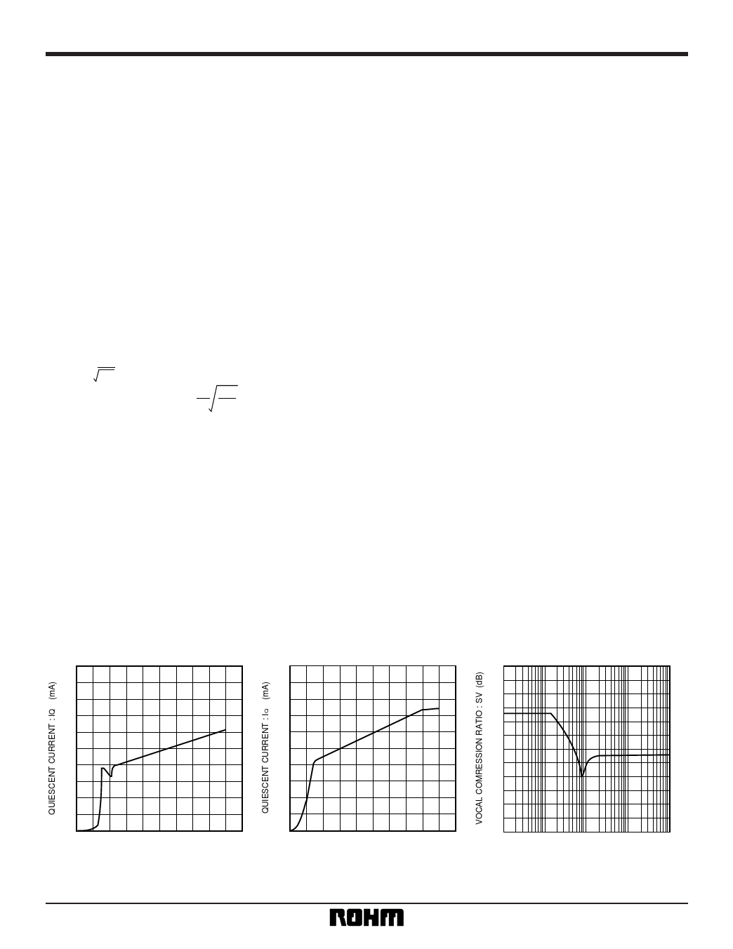
•Electrical characteristic curves
5
5
40
4
4
20
14
3
3
0
2
2
– 20
1
0 2 4 6 8 10 12 14 16 18 20
POWER SUPPLY VOLTAGE : VCC (V)
Fig. 3 IQ vs. VCC characteristics
(BA3837 / F)
10
1
0 2 4 6 8 10 12 14 16 18 20
POWER SUPPLY VOLTAGE : VCC (V)
Fig. 4 IQ vs. VCC characteristics
(BA3838F)
– 40
– 60
10
100
1K
10K
FREQUENCY : f (Hz)
100K
Fig. 5 SV vs. frequency
characteristics
Share Link: 