BA7645N データシートの表示(PDF) - ROHM Semiconductor
部品番号
コンポーネント説明
メーカー
BA7645N Datasheet PDF : 4 Pages
| |||
Multimedia ICs
BA7645N
•Measurement conditions
Parameter
Symbol
SW1
SW2
Switch settings
SW3 SW4 SW5
SW6
SW7
Measurement
method
Current dissipation
ICC
2
2
2
2
2
2
2
Ammeter
IN 1
Maximum
IN 2
output level IN 3
IN 4
Vom
Vom
Vom
Vom
1
2
2
2
2
1
2
2
2
2
1
2
2
2
2
1
3
3
2
2
3
2
3
2
3
3
3
3
f = 1kHz,
THD = 0.5%
Note 1
IN 1
Voltage gain
IN 2
IN 3
IN 4
GV
GV
GV
GV
1
2
2
2
1
2
2
2
1
2
2
2
2
2
2
1
3
3
2
2
3
2
3
2
3
3
3
3
f = 1MHz,
VIN = 1VP-P
Note 2
IN1→IN2
CT
1
2
2
2
3
2
3
IN1→IN3
CT
1
2
2
2
2
3
3
IN1→IN4
CT
1
2
2
2
2
2
3
Interchannel
crosstalk
IN1→MUTE
IN2→IN3
IN2→IN4
IN2→MUTE
CT
CT
CT
CT
1
2
2
2
1
2
2
1
2
2
1
2
2
2
2
2
∗
2
2
∗
∗
3
2
∗
2
3
3
2
f = 4.43MHz,
VIN = 1VP-P
Note 3
IN3→IN4
CT
2
2
1
2
2
2
3
IN3→MUTE
CT
2
2
1
2
∗
∗
2
IN4→MUTE
CT
2
2
2
1
∗
∗
2
IN 1
Frequency
IN 2
characteristic IN 3
IN 4
Gf
1
2
2
2
3
3
3 f = 10MHz /
Gf
2
1
2
2
3
2
3
1MHz
Gf
2
2
1
2
2
3
3
VIN = 1VP-P
Gf
2
2
2
1
2
2
3
Note 4
CTL pin
switching level
CTLA
CTLB
CTLC
VTH
2
2
1
2
1
3
3
VTH
2
1
2
2
3
1
3
VTH
1
2
2
2
3
3
1
Note 5
Note 6
∗ Anywhere is possible.
Note 1: Connect a distortion meter to the output, and input a f = 1kHz sine wave. Adjust the input level until the output distortion is 0.5%.
This output voltage at this time is the maximum output level Vom (VP-P).
Note 2: Input a f = 1MHz, VIN = 1VP-P sine wave. The voltage gain is given by GV = 20 log (VOUT / VIN).
Note 3: Input a f = 4.43MHz, VIN = 1VP-P sine wave. The interchannel crosstalk is given by CT = 20 log (VOUT / VIN).
Note 4: Input f = 1MHz and 10MHz, VIN = 1VP-P sine waves. The frequency characteristic is given by Gf = 20 log (VOUT (f = 10MHz) / VOUT (f = 1MHz)).
Note 5: Input a f = 1MHz, VIN = 1VP-P sine wave. Reduce the CTL pin voltage from VCC. The CTL pin switching level (VTH) is the CTL pin voltage at which
the VOUT level drops below 20mVP-P.
Note 6: Input a f = 1MHz, VIN = 1VP-P sine wave. Increase the CTL pin voltage from 0V. The CTL pin switching level (VTH) is the CTL pin voltage at which
the VOUT level goes below 1.0VDC
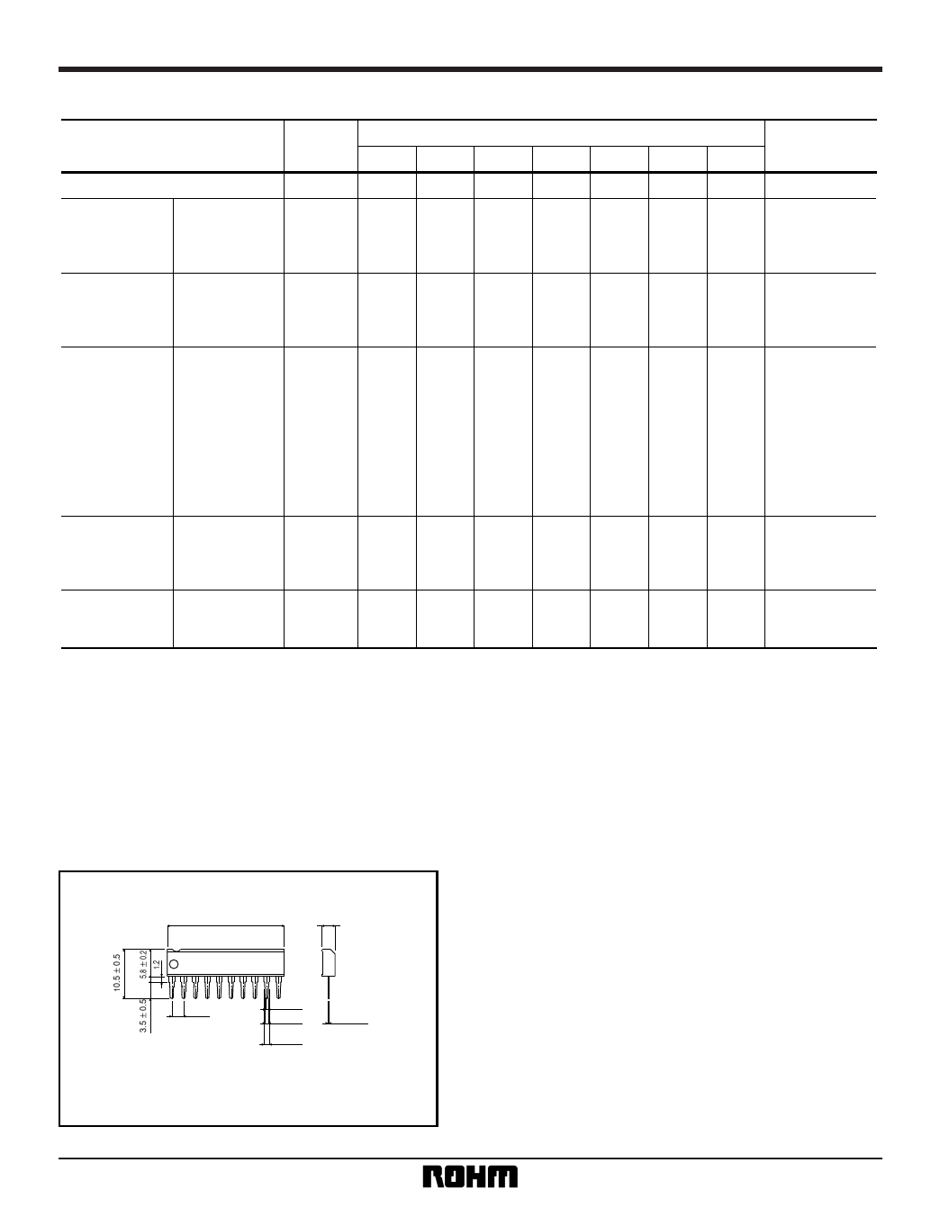
•External dimensions (Units: mm)
25.2 ± 0.2
2.8 ± 0.2
1
2.54
10
0.6
0.8
0.3 ± 0.1
1.3
SIP10
4
Share Link: 