AZ100EP16FELR2 データシートの表示(PDF) - AZ Microtek
部品番号
コンポーネント説明
メーカー
AZ100EP16FELR2
AZ Microtek

AZ100EP16FELR2 Datasheet PDF : 7 Pages
| |||
AZ100EP16FE
ARIZONA MICROTEK, INC.
FEATURES
• Silicon-Germanium for High Speed
Operation
• <100ps Typical Rise/Fall Times
• Optimized for 0.622 to 2.5Gbps Fiber
Applications
• Available in a 3x3mm MLP Package
ECL/PECL High Speed VCSEL Driver with
Variable Output Swing or Limiting Amplifier
PACKAGE AVAILABILITY
PACKAGE
MLP 8
MLP 8 T&R
MLP 8 T&R
TSSOP 8
TSSOP 8 T&R
TSSOP 8 T&R
PART NO.
AZ100EP16FEL
AZ100EP16FELR1
AZ100EP16FELR2
AZ100EP16FET
AZ100EP16FETR1
AZ100EP16FETR2
MARKING
AZM16D
AZM16D
AZM16D
AZHP16FE
AZHP16FE
AZHP16FE
DESCRIPTION
The AZ100EP16FE is a Silicon–Germanium (SiGe) differential VCSEL driver with variable output swing or
limiting post amplifier. The 100EP16FE is optimized for OC-12,OC-24, OC-48, Ethernet, Sonnet, Fiber Channel or
related applications at data rates up to 2.5Gbps. An input controls the amplitude of the Q/Q¯ outputs, which allows
compensation for differing VCSEL characteristics.
The operational range of the 100EP16FE control input, VCTRL, is from VREF (full swing) to VCC (small swing).
For post amplifier applications, maximum swing is achieved by leaving the VCTRL pin open or by tying it to the
negative supply pin (VEE). Simple control of the output swing can be obtained by a variable resistor between the
VREF and VCC pins, with the wiper driving VCTRL. A typical application circuit is described in this Data Sheet.
The 100EP16FE also provides a VREF output which functions as a DC bias for input AC coupling to the device.
The VREF pin should be used only as a bias for the 100EP16FE as its current sink/source capability is limited. When
used, the VREF pin should be bypassed to ground via a 0.01µF capacitor.
The maximum DC output current should be kept below 16mA. Connecting each output (Q/Q¯ ) to VEE with a
180Ω resistor is typically used. The load is then AC coupled from the output. DC and AC symmetrical loading of
the Q/Q¯ outputs will provide the best output wave shape.
Under open input conditions for D/D¯ , the Q/Q¯ outputs are not guaranteed.
NOTE: Specifications in ECL/PECL tables are valid when thermal equilibrium is established.
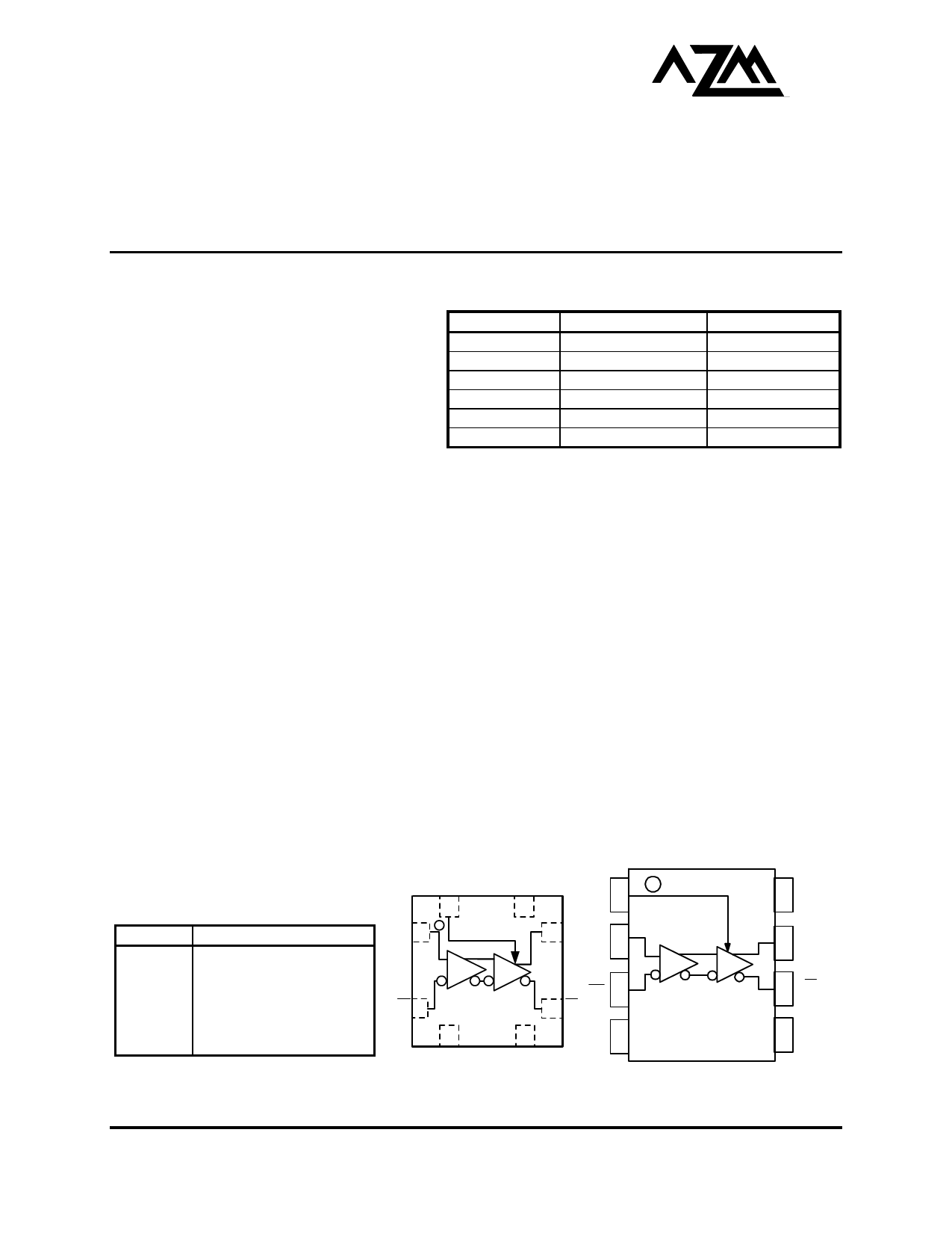
PIN DESCRIPTION
PIN
D, D¯
VCTRL
Q, Q¯
VREF
VCC
VEE
FUNCTION
Data Inputs
Output Swing Control
Data Outputs
Reference Voltage Output
Positive Supply
Negative Supply
VCTRL
8
D1
V CC
7
V CTRL 1
6Q D 2
D2
D3
5Q
3
V REF
4
V EE
VREF 4
8 MLP (TOP VIEW)
8 TSSOP
8 VCC
7Q
6Q
5 VEE
1630 S. STAPLEY DR., SUITE 125 • MESA, ARIZONA 85204 • USA • (480) 962-5881 • FAX (480) 890-2541
www.azmicrotek.com
Share Link: