BGX7100 データシートの表示(PDF) - NXP Semiconductors.
部品番号
コンポーネント説明
メーカー
BGX7100 Datasheet PDF : 38 Pages
| |||
NXP Semiconductors
12. Application information
BGX7100
Transmitter IQ modulator
100 nF
VCC
22 pF
modulator in-phase
positive input
modulator in-phase
negative input
24
POFF_P
1
LO input
1
5
O PRIMARY O
TC1-1-43A+
3
4
LOGND 2
18 pF LO_P 3
0.3 pF
LO_N 4
18 pF
LOGND
5
LOGND
6
7
23
22
21
20
19
VCC_RF(5V0)
18
VCC
BGX7100
RFGND
17
22 pF
100 nF
0°
90°
8
9
10
16 RFOUT
39 pF
RFOUTPUT
0.4 pF
15 i.c.
14 RFGND
13 i.c.
11
12
modulator quadrature
negative input
modulator quadrature
positive input
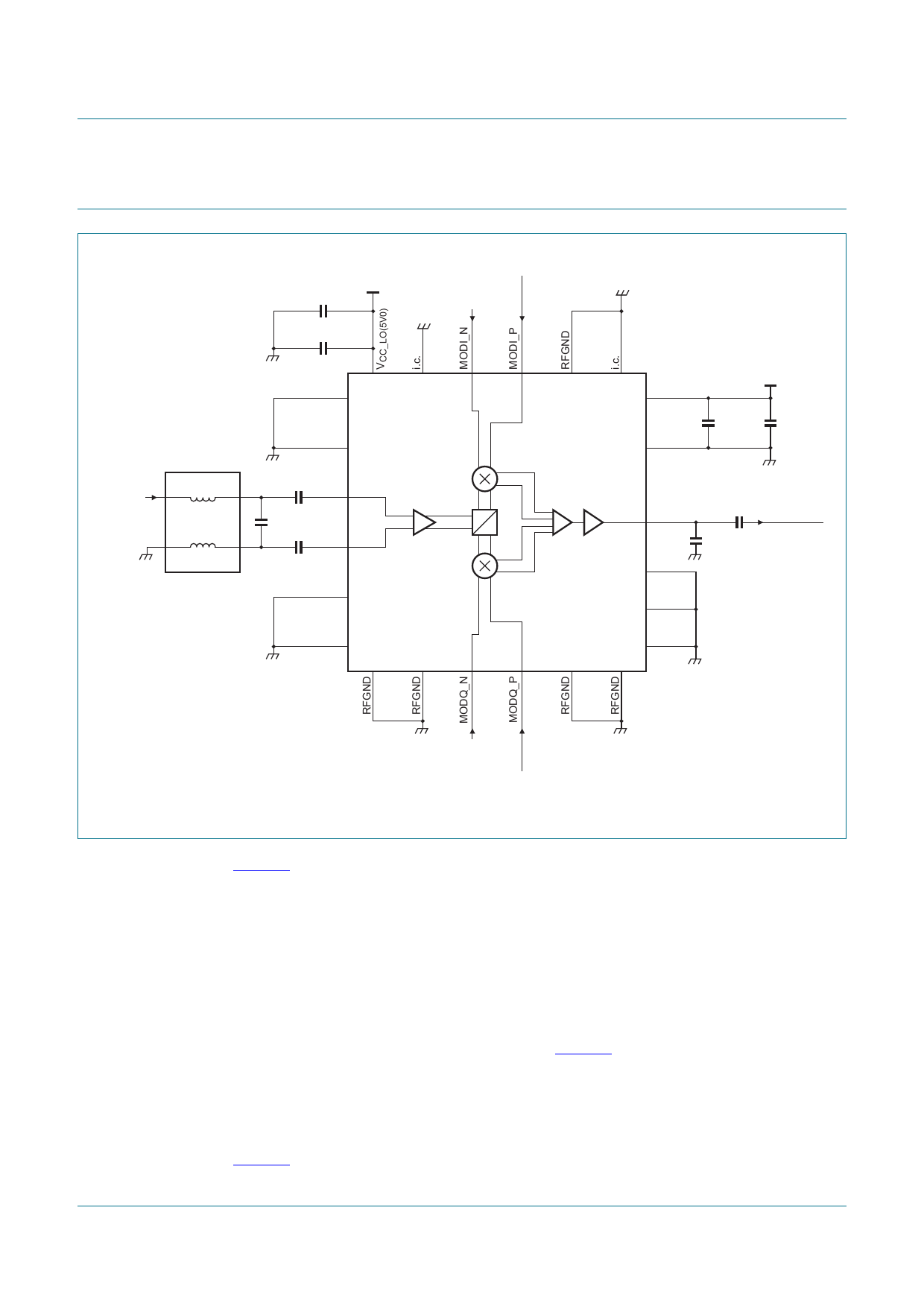
Fig 4. Typical wideband application diagram
aaa-002965
Figure 4 shows a typical wideband (from 0.4 GHz to 4 GHz) application circuit. Refer to
the application note for narrowband optimum component values.
12.1 External DAC interfacing
Nominal DAC single-ended output currents are between 0 mA and 20 mA.
If the DAC outputs are only designed for 1 V peak-to-peak differential (250 mV
peak-single) then the single-ended impedance at the DAC needs to be limited to 25 .
This can be split as 50 load resistors at the DAC outputs and a 225 differential
resistor in parallel to the modulator inputs (see Figure 5). In this way, the differential filter
can be properly terminated by 100 at both ends.
If the DAC outputs can withstand a higher swing without performance degradation, then
90 load resistors can be placed at the DAC outputs. No external resistors are needed in
this case, only the differential filter needs to be designed to have 180 at both ends (see
Figure 6).
BGX7100
Product data sheet
All information provided in this document is subject to legal disclaimers.
Rev. 5 — 3 September 2012
© NXP B.V. 2012. All rights reserved.
11 of 38
Share Link: 