BGX7100 データシートの表示(PDF) - NXP Semiconductors.
部品番号
コンポーネント説明
メーカー
BGX7100 Datasheet PDF : 38 Pages
| |||
NXP Semiconductors
BGX7100
Transmitter IQ modulator
5. Ordering information
Table 1. Ordering information
Type number
Package
Name
Description
BGX7100HN
HVQFN24 plastic thermal enhanced very thin quad flat package; no leads; 24
terminals; body 4 4 0.85 mm
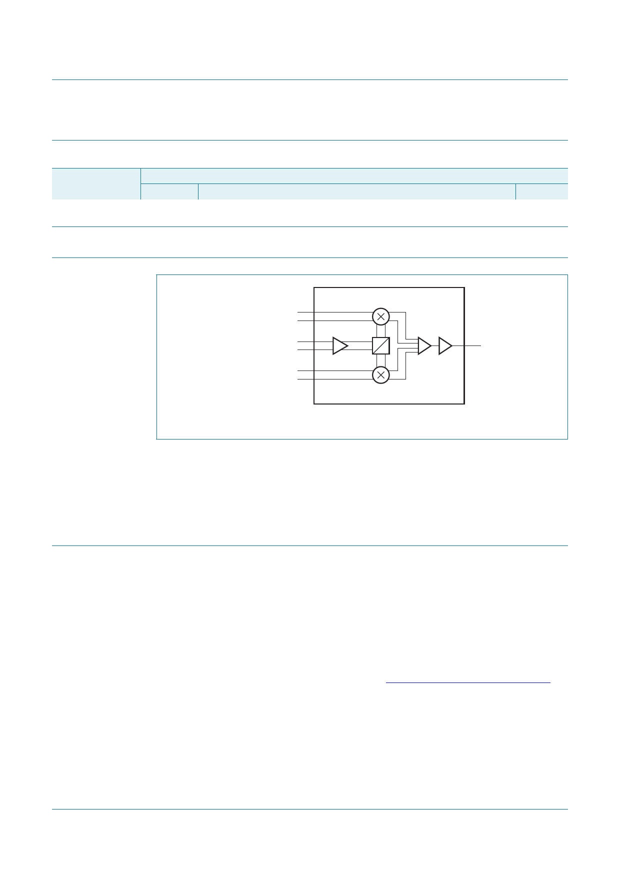
6. Functional diagram
Version
SOT616-3
I MODULATION IN
LOCAL OSCILLATOR IN
Q MODULATION IN
BGX7100
0°
90°
RF OUT
001aao016
Fig 1. Functional block diagram
Differential I and Q baseband inputs are each fed to an associated upconverter mixer. The
Local Oscillator (LO) carrier input is buffered and split into 0 degree and 90 degree
signals. The in-phase signal is passed to the I mixer and the 90 degree phase-changed
signal is passed to the Q mixer. The outputs of the mixers are summed to produce the
resulting RF output signal.
7. Pinning information
7.1 Pinning
The BGX7100 device pinout is designed to allow easy interfacing when mounted on a
Printed-Circuit Board (PCB). When viewing the device from above, the two differential IQ
baseband input paths are at the top and bottom. The common LO input is at the left and
the RF output at the right. Multiple power and ground pins allow for independent supply
domains, improving isolation between blocks. A small package footprint is chosen to
reduce bond-wire induced series inductance in the RF ports.
The input and output pin matching is described in Section 12 “Application information”.
BGX7100
Product data sheet
All information provided in this document is subject to legal disclaimers.
Rev. 5 — 3 September 2012
© NXP B.V. 2012. All rights reserved.
2 of 38
Share Link: 