BH3541F データシートの表示(PDF) - ROHM Semiconductor
部品番号
コンポーネント説明
メーカー
BH3541F Datasheet PDF : 9 Pages
| |||
BH3541F,BH3544F,BH3547F,BH3548F
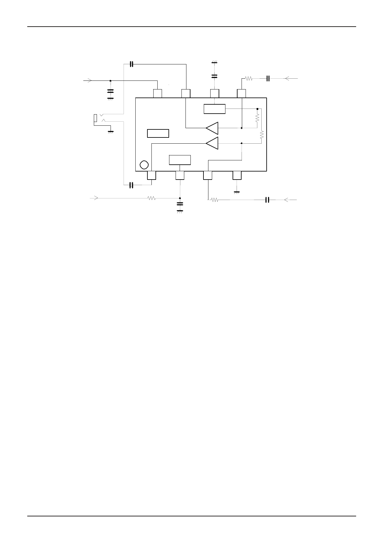
Technical Note
●Application circuit
C7
330 µ
+
C5
C6
R5
1µ
VCC
47µ
+
VIN2
C180µ +
VCC
8
OUT2
7
BIAS
6
IN2
5
TSD
BIAS
0dB
(6dB)
MUTE
0dB
(6dB)
180k
(90k)
180k
(90k)
VMUTE
H : Active
L : Mute
C1
330µ
+
1
OUT1
R2 100k
2
MUTE
C2
1µ
3
4
IN1
GND
C3
1µ
VIN1
R3
( ) are BH3544F, BH3547F, BH3548F values.
Fig. 15
●Description of external components.
1) Input coupling capacitors (C3, C5)
These are determined according to the lower cutoff frequency fc. Moreover, since lowering the capacitance can cause
the occurrence of pop noise, when changing this, determine it after adequate checking.
Since the input impedance of the BH3541F is 180kΩ and that of the BH3544F,BH3547F,BH3548F is 90kΩ, these are
found by the expressions below, although drift, temperature characteristics, and other considerations are necessary.
(Layered ceramic capacitors are recommended.)
C3(C5)=1/(2π×180kΩ×fc) [BH3541F]
C3(C5)=1/(2π× 90kΩ×fc) [BH3544F,BH3547F,BH3548F]
2) Bias capacitor (C6)
When VCC=5V, 47μF is recommended. Since lowering the capacitance too much can cause worsening of electrical
characteristics or the occurrence of pop noise, when changing this, determine it after checking this adequately.
3) Mute pin pop noise countermeasures (R2, C2)
Since the BH3541F,BH3544F,BH3548F has an impedance of 190kΩ against GND and the BH3547F has 200kΩ, it may
be impossible to cancel mute mode if R2 is made too large.
4) Output coupling capacitors (C1, C7)
These are determined by the lower cutoff frequency. If RL is the output load resistance (assuming a resistance RX is
put in for output protection or current restriction), these are found by the expression below.
C1(C7)=1/(2π×(RL+Rx)× fc)
5) Input gain adjustment resistances (R3, R5) (BH3544F,BH3547F)
Externally attached resistances (R3, R5) make input gain adjustment possible. The gain found by the expression
below can be set.
GVC=6+20log(90kΩ/(90kΩ+R3[R5])) [dB]
When input gain is not accommodated, these resistors have no use.
●Notes for use
1) Numbers and data in entries are representative design values and are not guaranteed values of the items.
2) Although we are confident in recommending the sample application circuits, carefully check their characteristics further
when using them. When modifying externally attached component constants before use, determine them so that they
have sufficient margins by taking into account variations in externally attached components and the Rohm LSI, not only
for static characteristics but also including transient characteristics.
3) Absolute maximum ratings
If applied voltage, operating temperature range, or other absolute maximum ratings are exceeded, the LSI may be
damaged. Do not apply voltages or temperatures that exceed the absolute maximum ratings. If you think of a case in
which absolute maximum ratings are exceeded, enforce fuses or other physical safety measures and investigate how
not to apply the conditions under which absolute maximum ratings are exceeded to the LSI.
www.rohm.com
© 2010 ROHM Co., Ltd. All rights reserved.
6/8
2010.05 - Rev.A
Share Link: 