BL3406B-18 データシートの表示(PDF) - Shanghai Belling Co., Ltd.
部品番号
コンポーネント説明
メーカー
BL3406B-18 Datasheet PDF : 11 Pages
| |||
BL3406B
1.5 MHz, 800mA Synchronous Buck Converter
Absolute Maximum Rating (Note 1)
Input Supply Voltage…………………-0.3V to +6V
RUN, VFB Voltages……………………-0.3V to +VIN
SW Voltages……………………-0.3V to (VIN+0.3V)
P-Channel Switch Source Current (DC) ………1A
N-Channel Switch Sink Current (DC) …………1A
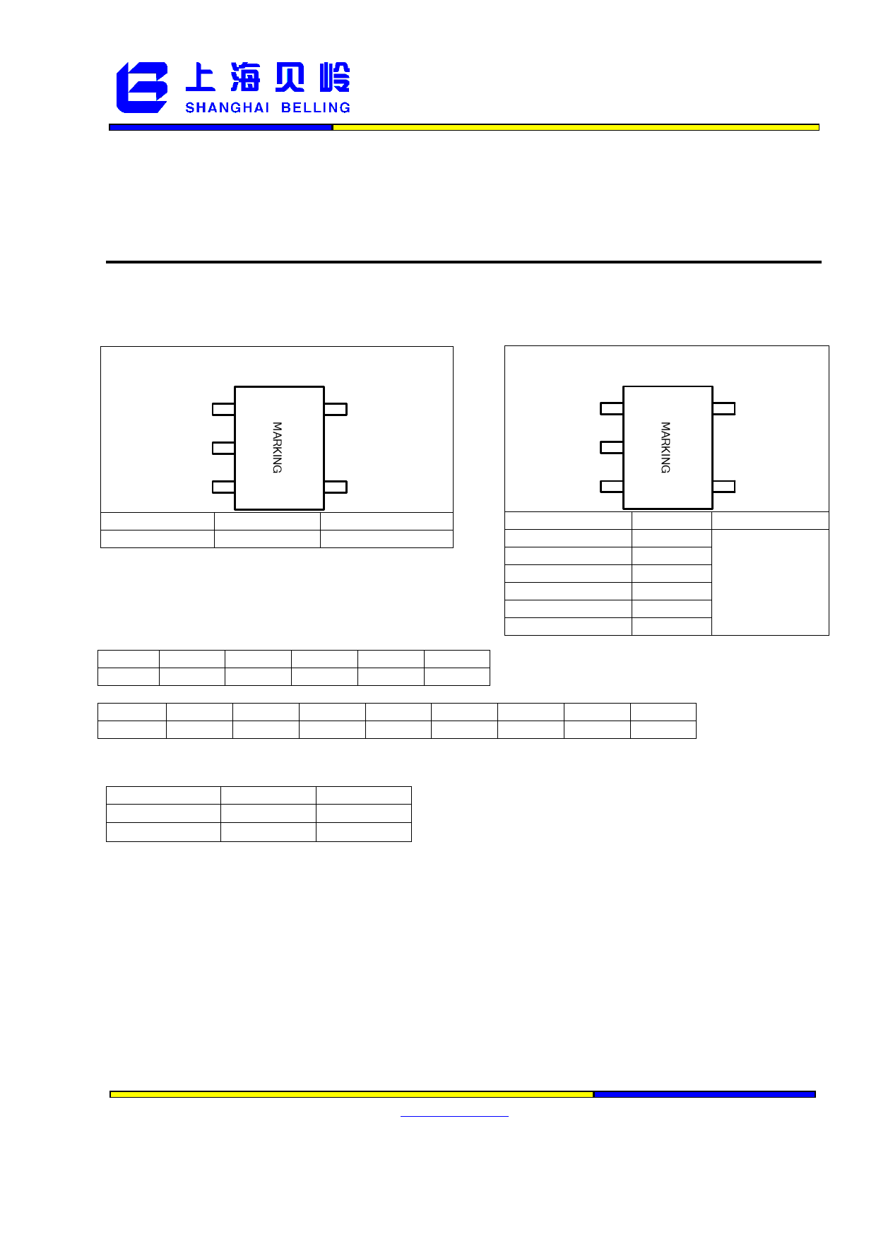
Package Information
Adjustable Output Version
Peak SW Sink and Source Current……………1.4A
Operating Temperature Range……-40°C to +85°C
Junction Temperature (Note2) ………………+125°C
Storage Temperature Range………-65°C to +150°C
Lead Temperature (Soldering, 10s) ………+300°C
Fixed Output Versions
SOT23-5
TOP VIEW
RUN 1
5 VFB
GND 2
SOT23-5
TOP VIEW
RUN 1
5 VOUT
GND 2
SW 3
4 VIN
Part Number
BL3406B-Adj
Top Mark
A J Y W(Note3)
Temp Range
-40°C to +85°C
Y
Year
9
2009
W
1
Week
A
A
2010
…
…
B
2011
26
Y
C
2012
27
Z
D
2013
28
a
SW 3
4 VIN
Part Number
BL3406B-1.0V
BL3406B-1.2V
BL3406B-1.5V
BL3406B-1.8V
BL3406B-2.5V
BL3406B-3.3V
Top Mark
AAYW
ABYW
ACYW
ADYW
AEYW
AFYW
Temp Range
-40°C to +85°C
…
53
54
…
y
z
Thermal Resistance (Note 4)
Package
TSOT23-5
ӨJA
220°C/W
ӨJC
110°C/W
SOT23-5
250°C/W
130°C/W
Note 1: Absolute Maximum Ratings are those values beyond which the life of a device may be impaired.
Note 2: TJ is calculated from the ambient temperature TA and power dissipation PD according to the following formula:
TJ = TA + (PD) x (220°C/W).
Note 3: Y: Year of wafer manufacturing W: Week of wafer manufacturing
Note 4: Thermal Resistance is specified with approximately 1 square of 1 oz copper.
PPMIC BU
www.belling.com.cn
2
BL3406B Rev 1.5
Belling Proprietary Information. Unauthorized Photocopy and Duplication Prohibited
10/2009
©2009 Belling All Rights Reserved
Share Link: 