MU9C2481L-10DC гғҮгғјгӮҝгӮ·гғјгғҲгҒ®иЎЁзӨәпјҲPDFпјү - Music Semiconductors
йғЁе“Ғз•ӘеҸ·
гӮігғігғқгғјгғҚгғігғҲиӘ¬жҳҺ
гғЎгғјгӮ«гғј
MU9C2481L-10DC Datasheet PDF : 20 Pages
| |||
LANCAM 1ST Family
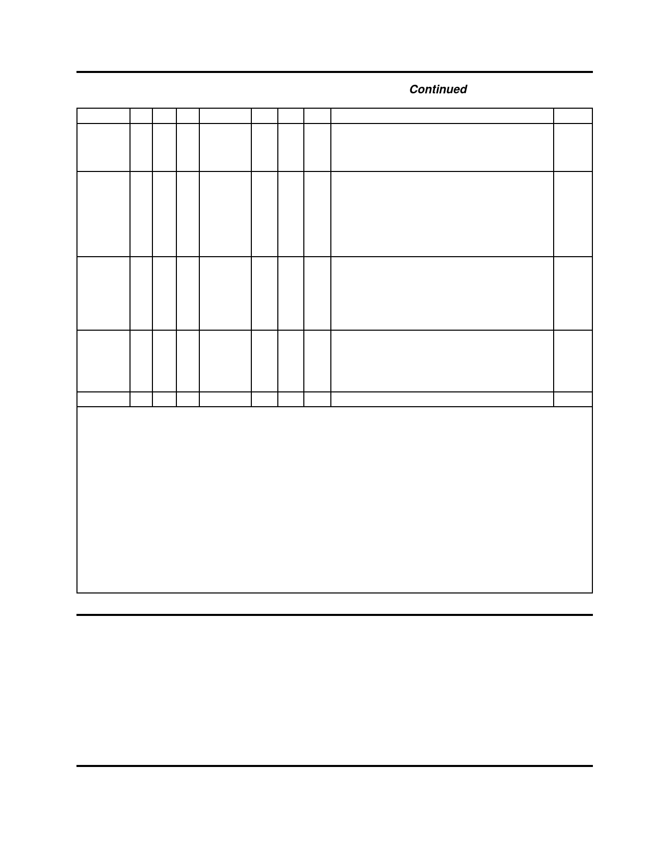
OPERATIONAL CHARACTERISTICS Continued
Cycle Type /E /CM /W I/O Status SPS SPD TCO Operation
Notes
Cmd Write L L L
IN
Load Instruction decoder
1
IN
Гј Load Address register
2,3
IN
Гј Load Control register
3
IN
Гј Load Segment Control register
3
Cmd Read L L H
OUT
Гј Read Next Free Address register
3
OUT
Гј Read Address register
3
OUT
Read Status Register bits 15вҖ“0
4
OUT
Read Status Register bits 31вҖ“16
5
Data Write L H L
OUT
OUT
OUT
IN
Гј Read Control register
3
Гј Read Segment Control register
3
Гј Read Current Persistent Source or Destination 3,10
Гј
Load Comparand register
6,9
IN
Гј
Load Mask Register 1
7,9
IN
Гј
Load Mask Register 2
7,9
IN
Гј
Write Memory Array at address
7,9
IN
Гј
Write Memory Array at Next Free address
7,9
IN
Гј
Write Memory Array at Highest-Priority match
7,9
Data Read L H H
OUT
Гј
Read Comparand register
6, 9
OUT
Гј
Read Mask Register 1
8, 9
OUT
Гј
Read Mask Register 2
8, 9
OUT
Гј
Read Memory Array at address
8, 9
OUT
Гј
Read Memory Array at Highest-Priority match 7, 8
H X X HIGH-Z
Deselected
Notes:
1. Default Command Write cycle destination (does not require a TCO instruction).
2. Default Command Write cycle destination (no TCO instruction required) if Address Field flag was set in bit 11 of the
instruction loaded in the previous cycle.
3. Loaded or read on the Command Write or Read cycle immediately following a TCO instruction. Active for one Command Write
or Read cycle only. NFA register cannot be loaded this way.
4. Default Command Read cycle source (does not require a TCO instruction).
5. Default Command Read cycle source (does not require a TCO instruction) if the previous cycle was a Command Read of
Status Register bits 15вҖ“0. If next cycle is not a Command Read cycle, any subsequent Command Read cycle will access the
Status Register bits 15вҖ“0.
6. Default persistent source and destination on power-up and after Reset. If other resources were sources or destinations,
SPD CR or SPS CR restores the Comparand register as the destination or source.
7. Selected by executing a Select Persistent Destination instruction.
8. Selected by executing a Select Persistent Source instruction.
9. Access may require multiple 16-bit Read or Write cycles. The Segment Control register is used to control the selection of the
desired 16-bit segment(s) by establishing the Segment countersвҖҷ start and end limits and count values.
10. A Command Read cycle after a TCO PS or TCO PD reads back the Instruction decoder bits that were last set to select a
persistant source or destination. The TCO PS instruction will also read back the Device ID.
Table 3: Input/Output Operations
Control Register bits CT3 and CT2 set the Address register to
automatically increment or decrement (or not change) during
sequences of Command or Data cycles. The Address register
will change after executing an instruction that includes
M@[AR] or M@aaaH, or after a data access to the end limit
segment (as set in the Segment Control register) when the
persistent source or destination is M@[AR] or M@aaaH.
Either the Foreground or Background Address register
will be active, depending on which register set has been
selected, and only the active Address register will be
written to or read from.
Next Free Address Register (NF)
The LANCAM 1ST automatically stores the address of the
first empty memory location in the Next Free Address register,
which is then used as a memory address pointer for M@NF
operations. The Next Free Address register, shown in Table 9
on page 16, can be read using a TCO NF instruction. After a
reset, the Next Free Address register is set to zero.
7
Rev. 1a
Share Link: 