Q67060-S6311 データシートの表示(PDF) - Infineon Technologies
部品番号
コンポーネント説明
メーカー
Q67060-S6311 Datasheet PDF : 15 Pages
| |||
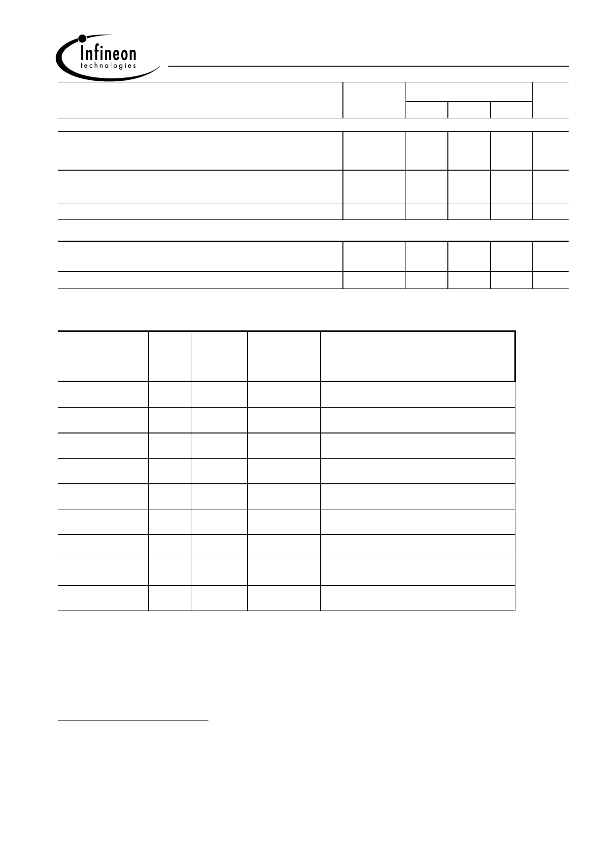
Data Sheet BTS6510
Parameter and Conditions
at Tj = -40 ... +150 °C, Vbb = 12 V unless otherwise specified
Symbol
Current sense leakage current
IIN = 0:
VIN = 0, IL ≤ 0:
Current sense overvoltage protection Tj =-40°C:
Ibb = 15 mA
Tj = 25...+150°C:
Current sense settling time20)
Input
Input and operating current (see diagram page 12)
IN grounded (VIN = 0)
Input current for turn-off21)
IIS(LL)
IIS(LH)
VbIS(Z)
ts(IS)
IIN(on)
IIN(off)
Values
Unit
min typ max
--
-- 0.5 µA
--
2
--
60
--
62 66
-- V
--
--
-- 500 µs
-- 0.8 1.5 mA
--
-- 80 µA
Truth Table
Normal
operation
Very high
load current
Current-
limitation
Short circuit to
GND
Over-
temperature
Short circuit to
Vbb
Open load
Negative output
voltage clamp
Inverse load
current
Input
current
level
L
H
H
H
L
H
L
H
L
H
L
H
L
L
H
Output
level
L
H
H
H
L
L
L
L
H
H
Z23)
H
L
H
H
Current
Sense
IIS
0
nominal
IIS, lim
0
0
0
0
0
0
<nominal 22)
0
0
0
0
0
Remark
=IL / kilis, up to IIS=IIS,lim
up to VON=VON(Fold back)
IIS no longer proportional to IL
VON > VON(Fold back)
L = "Low" Level
H = "High" Level
Overtemperature reset by cooling: Tj < Tjt (see diagram on page 14)
20) Not tested, specified by design.
21) We recommend the resistance between IN and GND to be less than 0.5 kΩ for turn-on and more than
500kΩ for turn-off. Consider that when the device is switched off (IIN = 0) the voltage between IN and GND
reaches almost Vbb.
22) Low ohmic short to Vbb may reduce the output current IL and can thus be detected via the sense current IIS.
23) Power Transistor "OFF", potential defined by external impedance.
Infineon Technologies AG
Page 6 of 15
2000-Mar-29
Share Link: 