BTS724G データシートの表示(PDF) - Infineon Technologies
部品番号
コンポーネント説明
メーカー
BTS724G Datasheet PDF : 16 Pages
| |||
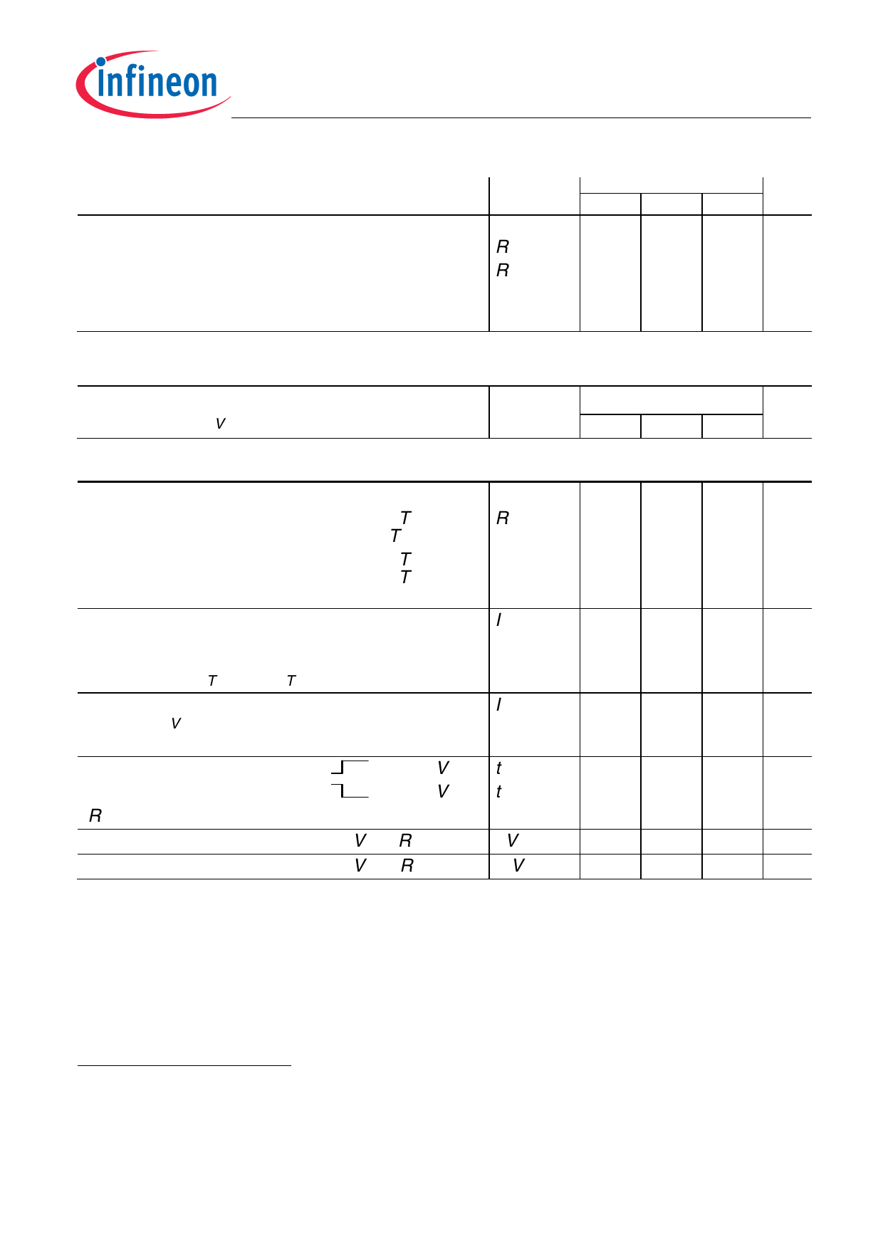
Smart High-Side Power Switch
BTS724G
Parameter and Conditions
Symbol
Thermal resistance
junction - soldering point6)7)
junction – ambient6)
@ 6 cm2 cooling area
each channel:
one channel active:
all channels active:
Rthjs
Rthja
Electrical Characteristics
Parameter and Conditions, each of the four channels
at Tj = -40...+150°C, Vbb = 12 V unless otherwise specified
Symbol
Load Switching Capabilities and Characteristics
On-state resistance (Vbb to OUT); IL = 2 A
each channel, Tj = 25°C: RON
Tj = 150°C:
two parallel channels, Tj = 25°C:
four parallel channels, Tj = 25°C:
see diagram, page 11
Nominal load current
one channel active: IL(NOM)
two parallel channels active:
four parallel channels active:
Device on PCB6), Ta = 85°C, Tj ≤ 150°C
Output current while GND disconnected or pulled up8); IL(GNDhigh)
Vbb = 32 V, VIN = 0,
see diagram page 9
Turn-on time9)
IN
to 90% VOUT: ton
Turn-off time
IN
to 10% VOUT: toff
RL = 12 Ω
Slew rate on 9)
Slew rate off 9)
10 to 30% VOUT, RL = 12 Ω: dV/dton
70 to 40% VOUT, RL = 12 Ω: -dV/dtoff
Values
Unit
min typ max
--
-- 15 K/W
-- 42
--
-- 34
--
Values
Unit
min typ max
-- 70 90 mΩ
-- 140 180
-- 35 45
-- 17.5 22.5
3.0 3.3
4.3 4.7
6.5 7.3
-- A
--
--
--
--
2 mA
-- 100 250 µs
-- 100 270
0.2
-- 1.0 V/µs
0.2
-- 1.1 V/µs
6) Device on 50mm*50mm*1.5mm epoxy PCB FR4 with 6cm2 (one layer, 70µm thick) copper area for Vbb
connection. PCB is vertical without blown air. See page 14
7) Soldering point: upper side of solder edge of device pin 15. See page 14
8) not subject to production test, specified by design
9) See timing diagram on page 12.
Data Sheet
5
V1.0, 2007-05-13
Share Link: 