ILC7070 データシートの表示(PDF) - Impala Linear Corporation
部品番号
コンポーネント説明
メーカー
ILC7070 Datasheet PDF : 6 Pages
| |||
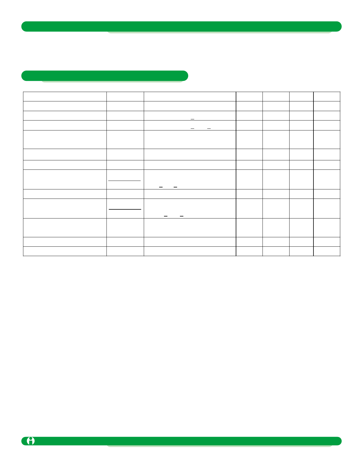
SOT-23 CMOS LDO Regulator with Shutdown
Electrical Characteristics ILC7070HCM-25
VOUT = 2.5V, TA = 25°C
Parameter
Output Voltage
Maximum Output Current
Load Stability
Input/Output
Voltage Differential
Supply Current 1
Supply Current 2
Input Stability
Input Voltage
Output Voltage
Temperature Characteristics
CE Input Current
CE ON Voltage
CE OFF Voltage
Symbol
VOUT
IOUTmax
∆VOUT
Vdif
Conditions
IOUT = 40mA, VIN = 3.5V
VIN = 3.5V, VOUT > 2.25V
VIN = 3.5V, 1mA < IOUT < 60mA
IOUT = 60mA, VOUT = VSET x .98
ISS1
ISS2
∆VOUT
∆VIN • VOUT
VIN
∆VOUT
∆Topr • VOUT
IIH
IIL
CE(ON)
CE(OFF)
VIN = VCE = 3.5V
VIN = 3.5V, VCE = open (Note 5)
IOUT = 40mA
3.5V< VIN < 10V
IOUT = 40mA
-30°C < Topr < 80°C
VIN = 3.5V, VCE = 3.5V
VIN = 3.5V, VCE = 0V
VIN = 3.5V
VIN = 3.5V
Min
2.450
125
2.5
0
Typ
2.5
45
180
5
0.5
0.2
±100
2
Max
2.55
90
360
Units
V
mA
mV
mV
10
µA
2
µA
0.3
%/V
10.0
V
ppm/°C
4
µA
0.1
VIN
V
0.7
V
Note:
1. VOUT means the output voltage when “VOUT + 1.0V” is provided at the VIN pin while maintaining a certain IOUT value.
2. VIN1 is defined as the input value that is gradually decreased until the output value reaches VOUT x 98%.
3. Vdif is defined as “VIN1-VOUT.”
4. IOUT: this is limited by continuous total power dissipation in the package.
5. When VCE is LOW or OPEN, the output is disabled.
Note: CE pin is a CMOS input. Because of this, when the input voltage reaches VIN/2, a rush current will start to flow.
Impala Linear Corporation
ILC7070 1.1
(408) 574-3939 www.impalalinear.com
Oct 1999 3
Share Link: 