LCX007BNB データシートの表示(PDF) - Sony Semiconductor
部品番号
コンポーネント説明
メーカー
LCX007BNB Datasheet PDF : 24 Pages
| |||
LCX007BNB
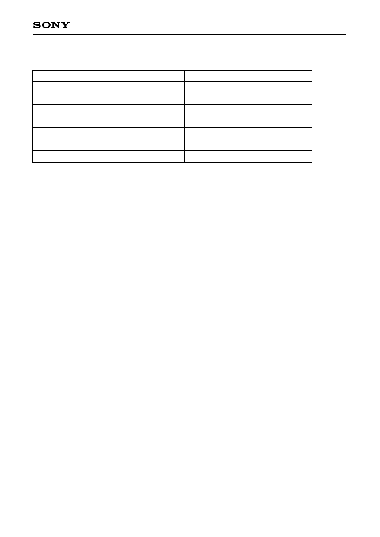
Input Signals
1. Input signal voltage conditions (VSS = 0V)
Item
Symbol Min.
Typ.
Max. Unit
H driver input voltage
(Low) VHIL
–0.5
0.0
WID, RGT, HST, HCK1, HCK2
(High) VHIH
4.5
5.0
0.3
V
5.5
V
V driver input voltage
(Low) VVIL
–0.5
0.0
CLR, ENB, VCK, PCG, VST, DWN (High) VVIH
4.5
5.0
0.3
V
5.5
V
Video signal center voltage
Video signal input range∗1
Common voltage of panel∗2
VVC
6.5
7.0
7.2
V
Vsig VVC – 4.5
—
VVC + 4.5 V
Vcom VVC – 0.5 VVC – 0.4 VVC – 0.3 V
∗1 Video input signal shall be symmetrical to VVC.
∗2 Common voltage of the panel shall be adjusted to VVC – 0.4V.
Level Conversion Circuit
The LCX007BNB has a built-in level conversion circuit in the clock input unit on the panel. The input signal
level increases to HVDD or VVDD. The VCC of external ICs are applicable to 5 ± 0.5V.
–5–
Share Link: 