PE9302-00 データシートの表示(PDF) - Unspecified
部品番号
コンポーネント説明
メーカー
PE9302-00 Datasheet PDF : 6 Pages
| |||
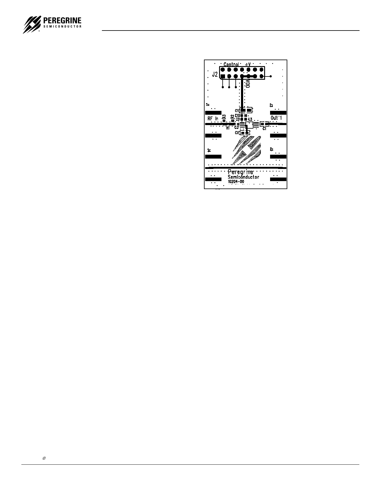
Evaluation Board Description
The PE9302 evaluation board is depicted in Figure
5. The input is driven into the RF In port while the
divided output is taken at Out 1. Both input and
output contain footprints for AC coupling capacitors
(C3 and C1 respectively). The power supply
connection is provided near the top of the
evaluation board, J2 Pin 1 as supply, J2 Pin 2 as
ground. In addition C2, C5, and C10 are
placeholders for power supply decoupling
capacitors. Placeholders C4, C6, and C8 are
needed for required bypass capacitors.
Note: C4 and C6 are located on the underside
of the evaluation board.
PE9302
Preliminary Specification
Figure 5. PE9302 Evaluation Board
Evaluation Board Test Setup
The PE9302 can be tested on the evaluation board
using the test setup shown in Figure 3 on page 3.
In the test setup, it is essential that the power
supply is properly decoupled and bypass
capacitors are used for pin 3. In addition, the input
and output need to be AC coupled.
Testing
The PE9302 Evaluation Board was measured prior
to shipment using the setup depicted in Figure 3.
Testing was performed at room temperature and
VDD = 2.85 V.
The input sensitivity plot for the PE9302 board is
included with the evaluation kit.
Applications Support
If you have a problem with your evaluation kit or if
you have applications questions call (858) 455-0660
and ask for applications support. You may also
contact us by fax or e-mail:
Fax: (858) 455-0770
E-Mail: help@peregrine-semi.com
Copyright Peregrine Semiconductor Corp. 2001
Page 4 of 6
File No. 70/0051~01A | UTSi CMOS RFIC SOLUTIONS
Share Link: 