RMPA0913C-58 データシートの表示(PDF) - Raytheon Company
部品番号
コンポーネント説明
メーカー
RMPA0913C-58 Datasheet PDF : 6 Pages
| |||
RMPA0913C-58
3.5V AMPS/CDMA Power Amplifier
Application
Information
PRODUCT INFORMATION
CAUTION: THIS IS AN ESD SENSITIVE DEVICE.
The following describes a procedure for evaluating the Raytheon RMPA0913C-58, a monolithic high efficiency
power amplifier, in a surface mount package, designed for use in the AMPS/CDMA dual mode portable phones.
Figure 1 shows the package outline and pin designations. Figure 2 shows the functional block diagram of the
packaged product. It should be noted that the amplifier requires external passive components for DC bias and RF
input and output matching circuits. A recommended schematic is shown in figure 3. The gate biases for the two
stages of the amplifier are set by simple on-chip circuits. Figure 4 shows a typical layout of an evaluation board
(RMPA0913C-58-TB), corresponding to the schematic circuit of figure 3. The following should be noted:
(1) Pin designations and their functions are as shown
in figure 1 and Table 1.
(2) Vg1, Vg2 are denoted as the Gate Voltages
(negative) applied at the pins of the package
(3) Vgg1, Vgg2 are denoted as the negative supply
voltages at the evaluation board terminals
(4) Vd1, Vd2 are denoted as the Drain Voltages
(positive) applied at the pins of the package
(5) Vdd1, Vdd2 are denoted as the positive supply
voltages at the evaluation board terminals
Note: The two drain voltages are tied to the same terminal denoted as Vdd on the evaluation board
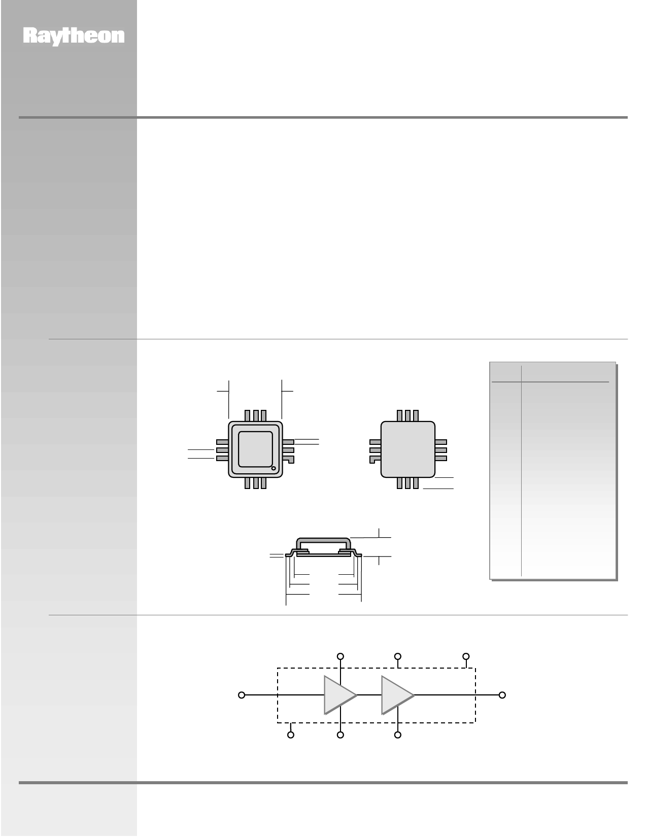
Figure 1
Package Information
Dimensions in inches
TOP VIEW
A
0.030
0.200 SQ.
6 54
7
RAY
3
8
RMBA
2
0913C-58
9
1
10
12
11
0.015
BOTTOM VIEW
45 6
3
7
2
13
8
1
9
12
10 0.041
11
0.010
PLASTIC LID
0.230
0.246
0.282
0.069 MAX.
SIDE SECTION
Pin # Description
1 RF Out & Vd2
2 RF Out & Vd2
3 RF Out & Vd2
4 AC Ground (g2)
5 GND
6 AC Ground (g1)
7 GND
8 RF Input
9 GND
10 Vd1
11 Vg2
12 Vg1
13 GND (METAL BASE)
Figure 2
Functional Block
Diagram of
Packaged Product
Vd1
Ground
AC Ground (g2)
Pin# 10 Pin# 5, 7, 9, 13
Pin# 4
RF IN
Pin# 8
RF OUT & Vd2
Pin# 1, 2, 3
www.raytheon.com/micro
AC Ground (g1) Vg1
Pin# 6 Pin# 12
Vg2
Pin# 11
Characteristic performance data and specifications are subject to change without notice.
Revised March 30, 2000
Page 2
Raytheon RF Components
362 Lowell Street
Andover, MA 01810
Share Link: 