3028A データシートの表示(PDF) - Harris Semiconductor
部品番号
コンポーネント説明
メーカー
3028A
Harris Semiconductor

3028A Datasheet PDF : 12 Pages
| |||
CA3028A, CA3028B, CA3053
Operating Conditions
Temperature Range . . . . . . . . . . . . . . . . . . . . . . . . . -55oC to 125oC
Thermal Information
Thermal Resistance (Typical, Note 1)
θJA (oC/W) θJC (oC/W)
Metal Can Package . . . . . . . . . . . . . . . 225
140
PDIP Package . . . . . . . . . . . . . . . . . . .
155
N/A
SOIC Package . . . . . . . . . . . . . . . . . . .
185
N/A
Maximum Junction Temperature (Metal Can Package) . . . . . . . 175oC
Maximum Junction Temperature (Plastic Package) . . . . . . . . 150oC
Maximum Storage Temperature Range . . . . . . . . . .-65oC to 150oC
Maximum Lead Temperature (Soldering 10s) . . . . . . . . . . . . 300oC
(SOIC - Lead Tips Only)
CAUTION: Stresses above those listed in “Absolute Maximum Ratings” may cause permanent damage to the device. This is a stress only rating and operation
of the device at these or any other conditions above those indicated in the operational sections of this specification is not implied.
NOTE:
1. θJA is measured with the component mounted on an evaluation PC board in free air.
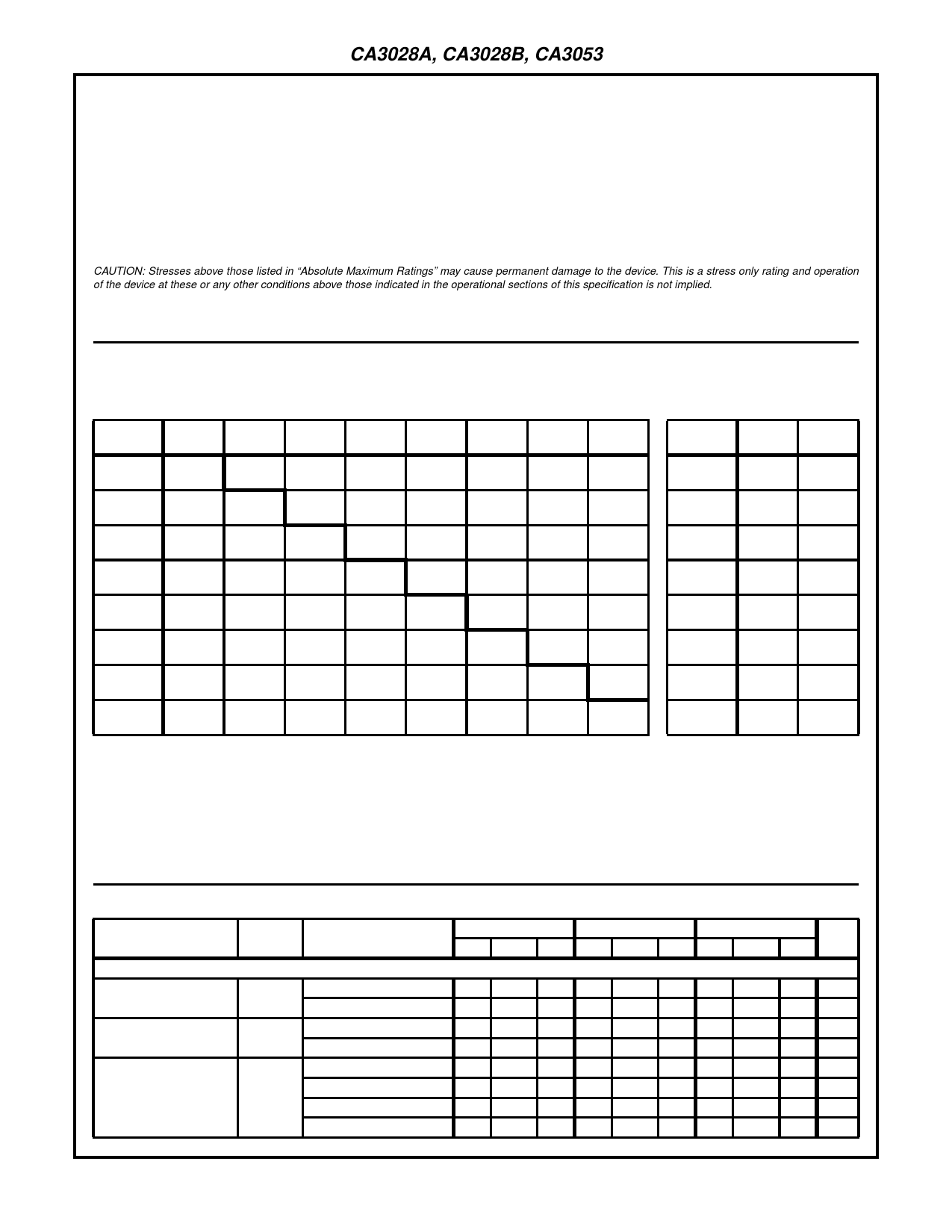
Absolute Maximum Voltage Ratings TA = 25oC
The following chart gives the range of voltages which can be applied to the terminals listed
horizontally with respect to the terminals listed vertically. For example, the voltage range of the
horizontal Terminal 4 with respect to Terminal 2 is -1V to +5V.
TERM
NO.
1
2
3
4
5
6
7
8
0 to -15 0 to -15 0 to -15 +5 to -5 Note 3 Note 3 +20 to 0
1
(Note 4) (Note 4) (Note 4)
(Note 5)
+5 to -11 +5 to -1 +15 to 0 Note 3 +15 to 0 Note 3
2
(Note 6)
(Note 6)
3
(Note 2)
+10 to 0 +15 to 0 +30 to 0 +15 to 0 +30 to 0
(Note 6) (Note 7) (Note 6) (Note 7)
+15 to 0 Note 3 Note 3 Note 3
4
(Note 6)
+20 to 0 Note 3 Note 3
5
(Note 5)
6
Note 3 Note 3
7
Note 3
8
NOTES:
2. Terminal No. 3 is connected to the substrate and case.
3. Voltages are not normally applied between these terminals. Voltages appearing between these
terminals will be safe, if the specified voltage limits between all other terminals are not exceeded.
4. Limit is -12V for CA3053.
5. Limit is +15V for CA3053.
6. Limit is +12V for CA3053.
7. Limit is +24V for CA3028A and +18V for CA3053.
Absolute Maximum
Current Ratings
TERM
IIN
IOUT
NO.
mA
mA
1
0.6
0.1
2
4
0.1
3
0.1
23
4
20
0.1
5
0.6
0.1
6
20
0.1
7
4
0.1
8
20
0.1
Electrical Specifications TA = 25oC
PARAMETER
SYMBOL TEST CONDITIONS
DC CHARACTERISTICS
Input Offset Voltage
(Figures 1, 14)
Input Offset Current
(Figures 2, 14)
Input Bias Current
(Figures 2, 3, 15, 16)
VIO VCC = 6V, VEE = -6V
VCC = 12V, VEE = -12V
IIO VCC = 6V, VEE = -6V
VCC = 12V, VEE = -12V
II
VCC = 6V, VEE = -6V
VCC = 12V, VEE = -12V
VCC = 9V
VCC = 12V
CA3028A
CA3028B
CA3053
MIN TYP MAX MIN TYP MAX MIN TYP MAX UNIT
-
-
-
- 0.98 5.0 -
-
-
-
- 0.89 5.0 -
-
-
-
- 0.56 5.0 -
-
-
-
- 1.06 6.0 -
- 16.6 70 - 16.6 40 -
-
36 106 -
36 80 -
-
-
-
-
-
-
-
-
-
-
-
-
-
-
- mV
-
- mV
-
- µA
-
- µA
-
- µA
-
- µA
29 85 µA
36 125 µA
7-7
Share Link: