CAT25010LA データシートの表示(PDF) - Catalyst Semiconductor => Onsemi
部品番号
コンポーネント説明
メーカー
CAT25010LA Datasheet PDF : 18 Pages
| |||
CAT25010, CAT25020, CAT25040
DESIGN CONSIDERATIONS
The CAT25010/20/40 powers up in a write disable state
and in a low power standby mode. A WREN instruction
must be issued to perform any writes to the device after
power up. After power up, CS must be brought low to
enter a ready state and receive an instruction. After a
successful byte/page write or status register write, the
CAT25010/20/40 goes into a write disable mode. CS
must be set high after the proper number of clock cycles
to start an internal write cycle. Access to the array
during an internal write cycle is ignored and program-
ming is continued. On power up, SO is in a high
impedance. If an invalid opcode is received, no data will
be shifted into the CAT25010/20/40, and the serial
output pin (SO) will remain in a high impedance state
until the falling edge of CS is detected again.
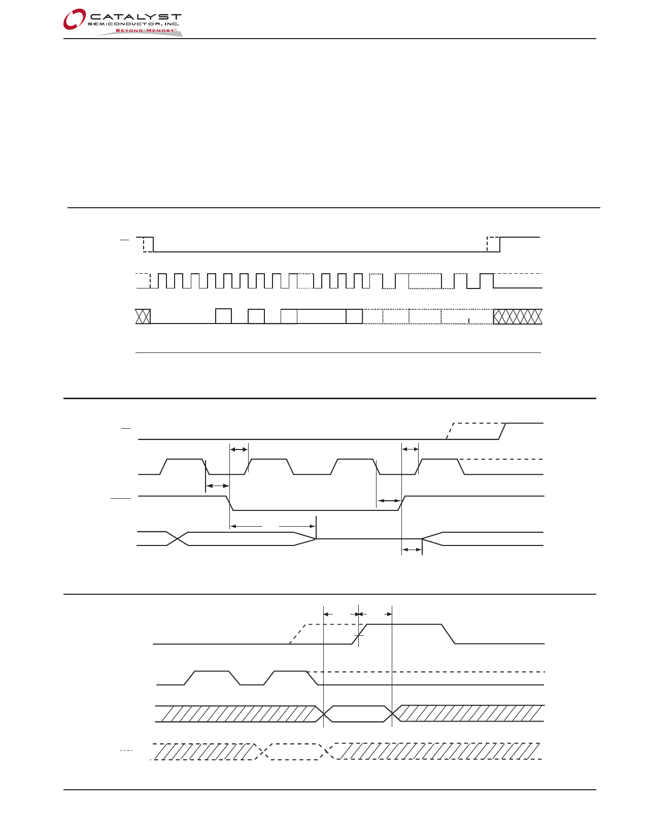
Figure 8. Page Write Instruction Timing
CS
SCK
SI
012345678
13 14 15 16-23 24-31 16+(N-1)x8-1..16+(N-1)x8 16+Nx8-1
OPCODE
0 0 0 0 X0* 0
BYTE ADDRESS
DATA IN
1 0 A7
Data Data Data
A0 Byte 1 Byte 2 Byte 3
Data Byte N
7..1
0
HIGH IMPEDANCE
SO
Note: Dashed Line= mode (1, 1) – – – – – *X=0 for 25010, 25020 ; X=A8 for 25040
Figure 9. HOLD Timing
CS
SCK
HOLD
SO
tCD
tHD
tHZ
Note: Dashed Line= mode (1, 1) – – – – –
tCD
tHD
HIGH IMPEDANCE
tLZ
Figure 10. WP Timing
CS
SCK
WP
WP
Note: Dashed Line= mode (1, 1) – – – – –
© 2006 by Catalyst Semiconductor, Inc.
Characteristics subject to change without notice
t WPS
t WPH
9
Doc. No. 1006, Rev. S
Share Link: 