CAT25010 データシートの表示(PDF) - Catalyst Semiconductor => Onsemi
部品番号
コンポーネント説明
メーカー
CAT25010 Datasheet PDF : 17 Pages
| |||
CAT25010, CAT25020, CAT25040
PIN DESCRIPTION
SI: The serial data input pin accepts op-codes,
addresses and data. In SPI modes (0,0) and (1,1)
input data is latched on the rising edge of the SCK
clock input.
SO: The serial data output pin is used to transfer data
out of the device. In SPI modes (0,0) and (1,1) data is
shifted out on the falling edge of the SCK clock.
SCK: The serial clock input pin accepts the clock
provided by the host and used for synchronizing
communication between host and CAT25010/20/40.
C¯¯S: The chip select input pin is used to enable/disable
the CAT25010/20/40. When C¯¯S is high, the SO output
is tri-stated (high impedance) and the device is in
Standby Mode (unless an internal write operation is in
progress). Every communication session between host
and CAT25010/20/40 must be preceded by a high to
low transition and concluded with a low to high
transition of the C¯¯S input.
¯W¯P¯: The write protect input pin will allow all write
operations to the device when held high. When ¯W¯P¯
pin is tied low all write operations are inhibited.
H¯¯O¯L¯D¯: The ¯H¯O¯L¯D¯ input pin is used to pause trans–
mission between host and CAT25010/20/40, without
having to retransmit the entire sequence at a later
time. To pause, H¯¯O¯L¯D¯ must be taken low and to
resume it must be taken back high, with the SCK
input low during both transitions. When not used for
pausing, the ¯H¯O¯L¯D¯ input should be tied to VCC,
either directly or through a resistor.
FUNCTIONAL DESCRIPTION
The CAT25010/20/40 devices support the Serial
Peripheral Interface (SPI) bus protocol, modes (0,0)
and (1,1). The device contains an 8-bit instruction
register. The instruction set and associated op-codes
are listed in Table 1.
Reading data stored in the CAT25010/20/40 is accom–
plished by simply providing the READ command and an
address. Writing to the CAT25010/20/40, in addition to
a WRITE command, address and data, also requires
enabling the device for writing by first setting certain bits
in a Status Register, as will be explained later.
After a high to low transition on the C¯¯S input pin, the
CAT25010/20/40 will accept any one of the six
instruction op-codes listed in Table 1 and will ignore all
other possible 8-bit combinations. The communication
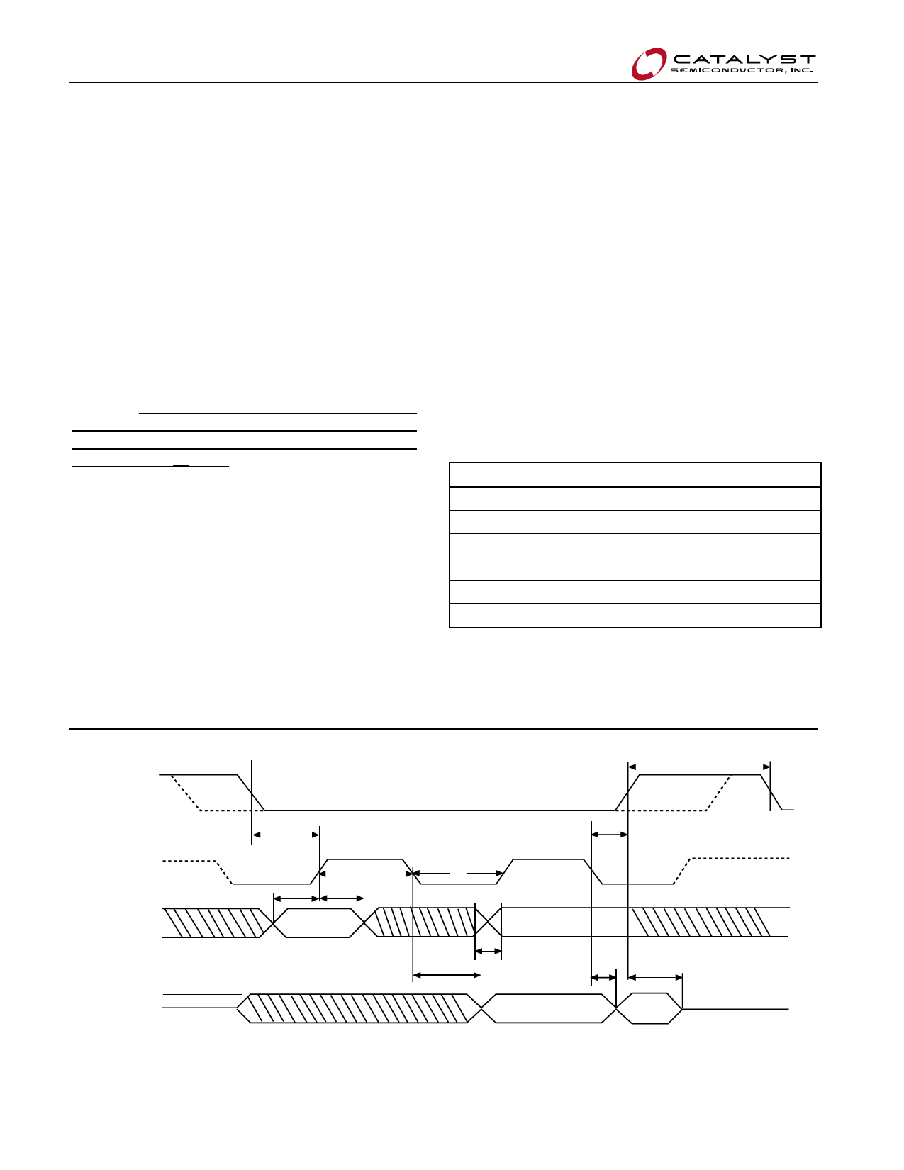
protocol follows the timing from Figure 1.
Table 1: Instruction Set (1)
Instruction Opcode Operation
WREN
WRDI
RDSR
WRSR
READ
WRITE
0000 0110
0000 0100
0000 0101
0000 0001
0000 X011
0000 X010
Enable Write Operations
Disable Write Operations
Read Status Register
Write Status Register
Read Data from Memory
Write Data to Memory
Note:
(1) X = 0 for CAT25010, CAT25020. X = A8 for CAT25040
Figure 1. Synchronous Data Timing
VIH
CS
VIL
VIH
SCK
VIL
VIH
SI
VIL
tCSS
tWH
tSU
tH
VALID IN
VOH
SO
HI-Z
VOL
Note: Dashed Line = mode (1, 1) - - - - - -
© Catalyst Semiconductor, Inc.
Characteristics subject to change without notice
tCS
tCSH
tWL
tRI
tFI
tV
tHO
tDIS
HI-Z
4
Doc. No. MD-1006 Rev. T
Share Link: 