CAT25C03GL データシートの表示(PDF) - Catalyst Semiconductor => Onsemi
部品番号
コンポーネント説明
メーカー
CAT25C03GL Datasheet PDF : 12 Pages
| |||
CAT25C11/03/05/09/17
1K/2K/4K/8K/16K SPI Serial CMOS EEPROM
FEATURES
s 10 MHz SPI compatible
s 1.8 to 6.0 volt operation
s Hardware and software protection
s 1,000,000 program/erase cycles
s 100 year data retention
s Self-timed write cycle
s Low power CMOS technology
s 8-pin DIP/SOIC, 8-pin TSSOP and 8-pin MSOP
s SPI modes (0,0 & 1,1)*
s Commercial, industrial, automotive and extended
temperature ranges
ts DESCRIPTION
The CAT25C11/03/05/09/17 is a 1K/2K/4K/8K/16K-Bit
r SPI Serial CMOS EEPROM internally organized as
128x8/256x8/512x8/1024x8/2048x8 bits. Catalyst’s
a advanced CMOS Technology substantially reduces
device power requirements. The CAT25C11/03/05
P features a 16-byte page write buffer. The 25C09/17
features a 32-byte page write buffer.The device operates
via the SPI bus serial interface and is enabled though a
Chip Select (CS). In addition to the Chip Select, the clock
s 16/32-byte page write buffer
s Write protection
– Protect first page, last page, any 1/4 array or
lower 1/2 array
input (SCK), data in (SI) and data out (SO) are required
to access the device. The HOLD pin may be used to
suspend any serial communication without resetting the
serial sequence. The CAT25C11/03/05/09/17 is designed
with software and hardware write protection features
including Block Write protection. The device is available
in 8-pin DIP, 8-pin SOIC, 8/14-pin TSSOP and 8-pin
MSOP packages.
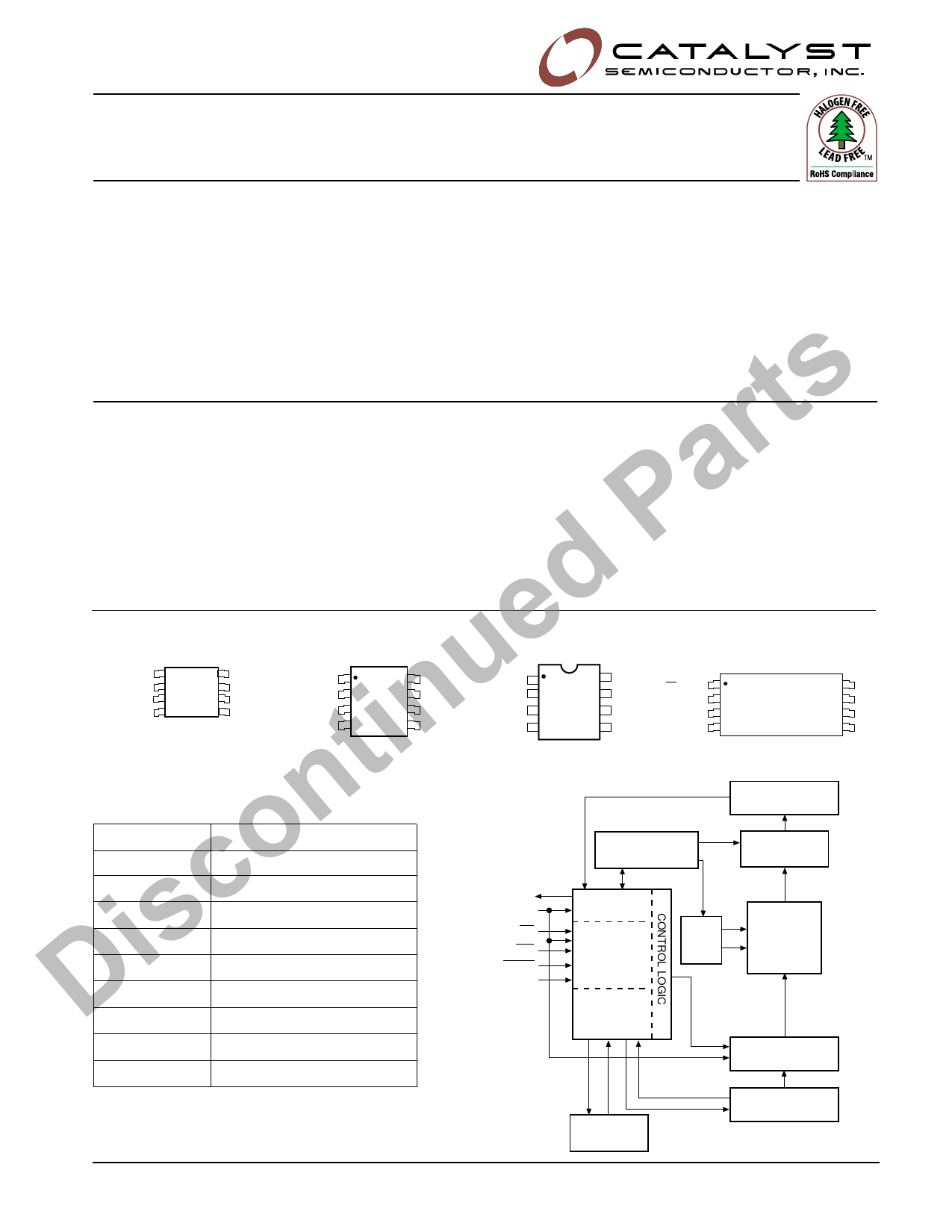
d PIN CONFIGURATION
e MSOP Package (R, Z, GZ)* SOIC Package (S, V, GV)
CS 1
u SO 2
WP 3
VSS 4
8 VCC
7 HOLD
6 SCK
5 SI
tin *CAT25C11/03 only
CS 1
SO 2
WP 3
VSS 4
8 VCC
7 HOLD
6 SCK
5 SI
DIP Package (P, L, GL)
CS 1
SO 2
WP 3
VSS 4
8 VCC
7 HOLD
6 SCK
5 SI
TSSOP Package (U, Y, GY)
CS
1
SO 2
WP 3
VSS
4
8
VCC
7
HOLD
6
SCK
5 SI
PIN FUNCTIONS
n Pin Name
Function
o SO
SCK
Serial Data Output
Serial Clock
c WP
Write Protect
isVCC
+1.8V to +6.0V Power Supply
VSS
Ground
CS
Chip Select
DSI
Serial Data Input
BLOCK DIAGRAM
SENSE AMPS
SHIFT REGISTERS
WORD ADDRESS
BUFFERS
COLUMN
DECODERS
SO
SI
CS
WP
HOLD
SCK
I/O
CONTROL
SPI
CONTROL
LOGIC
BLOCK
PROTECT
LOGIC
XDEC
EEPROM
ARRAY
HOLD
NC
Suspends Serial Input
No Connect
DATA IN
STORAGE
* Other SPI modes available on request.
STATUS
REGISTER
HIGH VOLTAGE/
TIMING CONTROL
© 2005 by Catalyst Semiconductor, Inc.
Characteristics subject to change without notice
1
Doc. No. 1017, Rev. L
Share Link: 