CAT25C03GL データシートの表示(PDF) - Catalyst Semiconductor => Onsemi
部品番号
コンポーネント説明
メーカー
CAT25C03GL Datasheet PDF : 12 Pages
| |||
CAT25C11/03/05/09/17
FUNCTIONAL DESCRIPTION
the operation to be performed.
The CAT25C11/03/05/09/17 supports the SPI bus data
transmission protocol. The synchronous Serial Periph-
eral Interface (SPI) helps the CAT25C11/03/05/09/17 to
interface directly with many of today’s popular
microcontrollers. The CAT25C11/03/05/09/17 contains
an 8-bit instruction register. (The instruction set and the
operation codes are detailed in the instruction set table)
PIN DESCRIPTION
SI: Serial Input
SI is the serial data input pin. This pin is used to input all
opcodes, byte addresses, and data to be written to the
25C11/03/05/09/17.Input data is latched on the rising
edge of the serial clock for SPI modes (0, 0 & 1, 1).
After the device is selected with CS going low, the first
SO: Serial Output
byte will be received. The part is accessed via the SI pin,
SO is the serial data output pin. This pin is used to transfer
with data being clocked in on the rising edge of SCK.
The first byte contains one of the six op-codes that define
data out of the 25C11/03/05/09/17. During a read cycle,
data is shifted out on the falling edge of the serial clock for
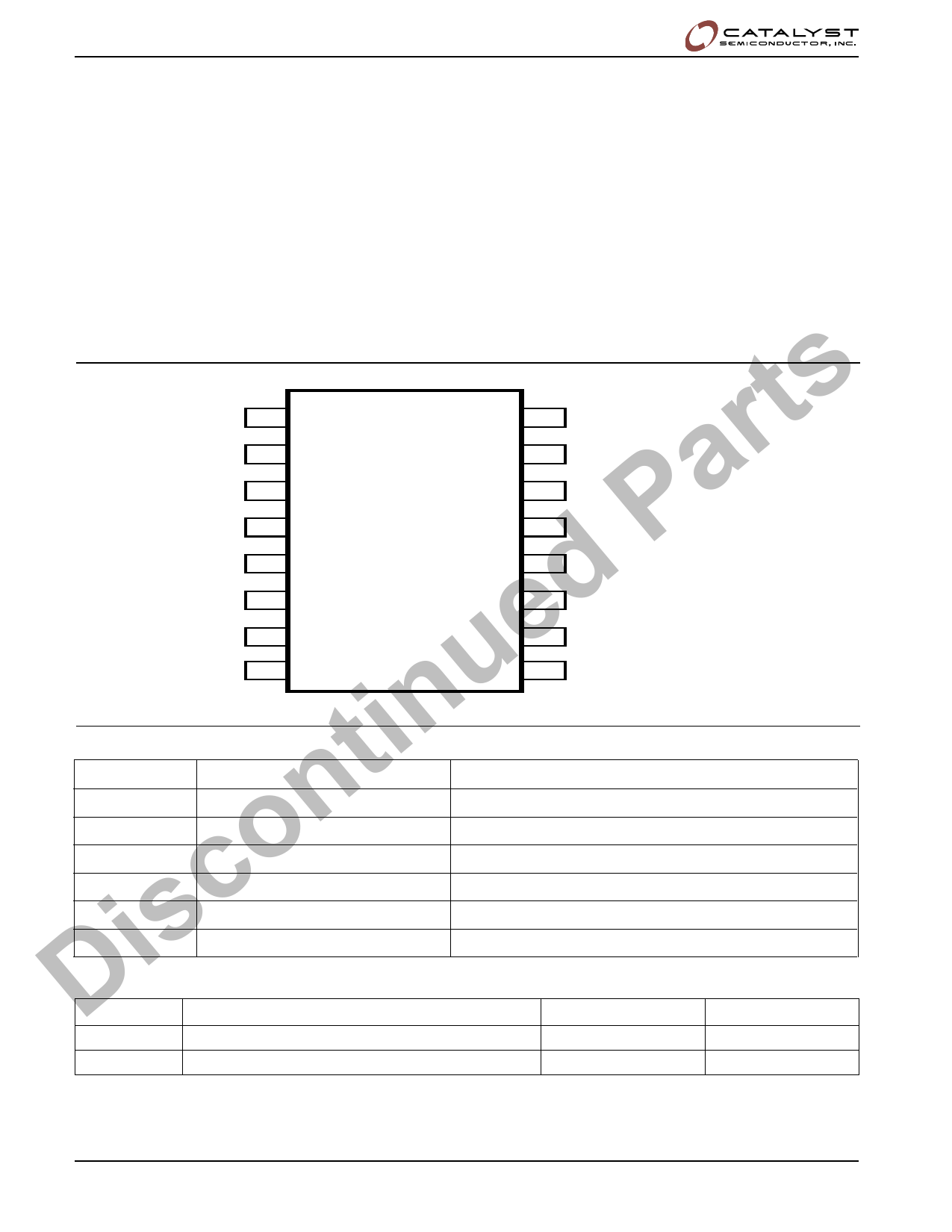
Figure 1. Sychronous Data Timing
ts CS
1
r SO
2
a NC
3
NC
4
P NC
5
d NC
6
e WP
7
VSS
8
u Note: Dashed Line= mode (1, 1) – – – –
16
15
14
13
12
11
10
9
VCC
HOLD
NC
NC
NC
NC
SCK
SI
tin INSTRUCTION SET
Instruction
WREN
n WRDI
RDSR
o WRSR
c READ
isWRITE
Opcode
0000 0110
0000 0100
0000 0101
0000 0001
0000 X011(1)
0000 X010(1)
Operation
Enable Write Operations
Disable Write Operations
Read Status Register
Write Status Register
Read Data from Memory
Write Data to Memory
Power-Up Timing(2)(3)
DSymbol
Parameter
Max.
Units
tPUR
Power-up to Read Operation
1
ms
tPUW
Power-up to Write Operation
1
ms
Note:
(1) X=0 for 25C11, 25C03, 25C09, 25C17. X=A8 for 25C05
(2) This parameter is tested initially and after a design or process change that affects the parameter.
(3) tPUR and tPUW are the delays required from the time VCC is stable until the specified operation can be initiated.
Doc. No. 1017, Rev. L
4
© 2005 by Catalyst Semiconductor, Inc.
Characteristics subject to change without notice
Share Link: 