CAT6218(2009) データシートの表示(PDF) - ON Semiconductor
部品番号
コンポーネント説明
メーカー
CAT6218 Datasheet PDF : 9 Pages
| |||
CAT6218
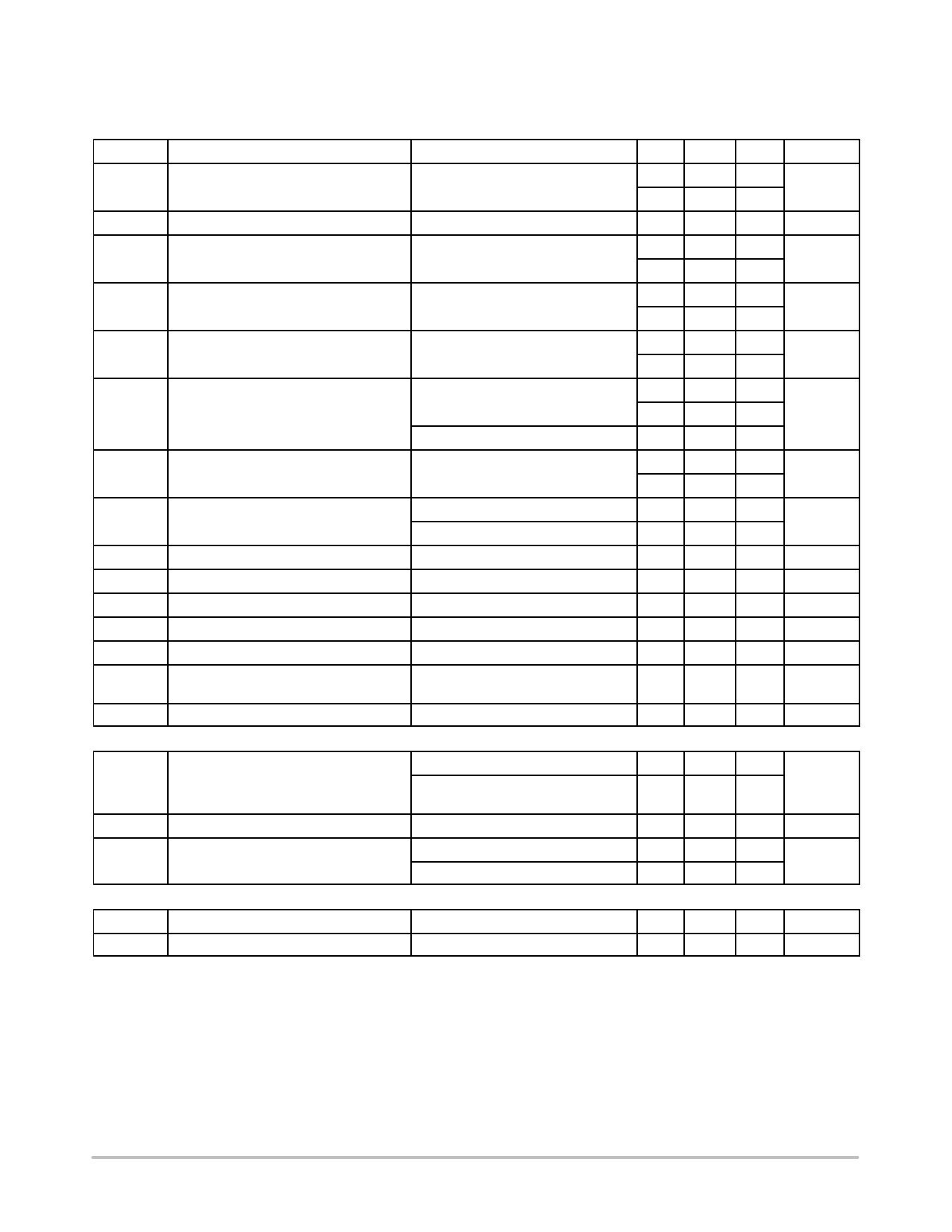
Table 3. ELECTRICAL OPERATING CHARACTERISTICS (Note 3)
(VIN = VOUT + 1.0 V, VEN = High, IOUT = 100 mA, CIN = COUT = 1 mF, ambient temperature of 25°C (over recommended operating
conditions unless specified otherwise). Bold numbers apply for the entire junction temperature range.)
Symbol
Parameter
Conditions
Min Typ Max
Unit
VOUT−ACC Output Voltage Accuracy
Initial accuracy for VOUT ≥ 2.0 V
(Note 6)
−1.0
−2.0
+1.0
%
+2.0
TCOUT
VR−LINE
Output Voltage Temp. Coefficient
Line Regulation
VIN = VOUT + 1.0 V to 5.5 V
40
−0.2 ±0.1 +0.2
−0.4
+0.4
ppm/°C
%/V
VR−LOAD Load Regulation
IOUT = 100 mA to 300 mA
0.7
1.2
%
1.5
VDROP Dropout Voltage (Note 4)
IOUT = 300 mA
180 250
mV
300
IGND
Ground Current
IOUT = 0 mA
55
75
mA
90
IGND−SD Shutdown Ground Current
IOUT = 300 mA
VEN < 0.4 V
80
1
mA
2
PSRR Power Supply Rejection Ratio
ISC
TON
eN
ROUT−SH
REN
VUVLO
Output short circuit current limit
Turn−On Time
Output Noise Voltage (Note 5)
Shutdown Switch Resistance
Enable pull−down resistor
Under−voltage lock out (UVLO)
threshold
f = 1 kHz, CBYP = 10 nF
f = 20 kHz, CBYP = 10 nF
VOUT = 0 V
CBYP = 10 nF
BW = 10 Hz to 100 kHz
64
dB
54
180
mA
150
ms
45
mVrms
250
W
2.5
MW
2.1
V
ESR
COUT equivalent series resistance
ENABLE INPUT
5
500
mW
VHI
Logic High Level
VIN = 2.3 to 5.5 V
1.8
V
VIN = 2.3 to 5.5 V, 0°C to +125°C
1.6
junction temperature
VLO
Logic Low Level
IEN
Enable Input Current
THERMAL PROTECTION
VIN = 2.3 to 5.5 V
VEN = 0.4 V
VEN = VIN
0.4
V
0.15
1
mA
1.5
4
TSD
Thermal Shutdown
160
°C
THYS
Thermal Hysteresis
10
°C
3. Specification for 2.80 V output version unless specified otherwise.
4. Dropout voltage is defined as the input−to−output differential at which the output voltage drops 2% below its nominal value measured at 1 V
differential. During test, the input voltage stays always above the minimum 2.3 V.
5. Specification for 1.8 V output version.
6. For VOUT < 2.0 V, the initial accuracy is ±2% and across temperature ±3%.
http://onsemi.com
3
Share Link: 