CDP1802A データシートの表示(PDF) - Intersil
部品番号
コンポーネント説明
メーカー
CDP1802A Datasheet PDF : 28 Pages
| |||
CDP1802A, CDP1802AC, CDP1802BC
Absolute Maximum Ratings
Thermal Information
DC Supply Voltage Range, (VDD)
(All Voltages Referenced to VSS Terminal)
CDP1802A. . . . . . . . . . . . . . . . . . . . . . . . . . . . . . . . . -0.5V to +11V
CDP1802AC, CDP1802BC. . . . . . . . . . . . . . . . . . . . -0.5V to +7V
Input Voltage Range, All Inputs . . . . . . . . . . . . . .-0.5V to VDD +0.5V
DC Input Current, any One Input . . . . . . . . . . . . . . . . . . . . . . . . . ±10mA
Thermal Resistance (Typical, Note 4)
θJA (oC/W) θJC (oC/W)
PDIP . . . . . . . . . . . . . . . . . . . . . . . . . .
50
N/A
PLCC . . . . . . . . . . . . . . . . . . . . . . . . . .
46
N/A
SBDIP . . . . . . . . . . . . . . . . . . . . . . . . .
55
15
Device Dissipation Per Output Transistor
TA = Full Package Temperature Range . . . . . . . . . . . . . . . 100mW
Operating Temperature Range (TA)
Package Type D . . . . . . . . . . . . . . . . . . . . . . . . . . -55oC to +125oC
Package Type E and Q. . . . . . . . . . . . . . . . . . . . . . -40oC to +85oC
Storage Temperature Range (TSTG) . . . . . . . . . . . . -65oC to +150oC
Lead Temperature (During Soldering)
At distance 1/16 ± 1/32 In. (1.59 ± 0.79mm)
from case for 10s max . . . . . . . . . . . . . . . . . . . . . . . . . . . . +265oC
Lead Tips Only. . . . . . . . . . . . . . . . . . . . . . . . . . . . . . . . . . +300oC
CAUTION: Stresses above those listed in “Absolute Maximum Ratings” may cause permanent damage to the device. This is a stress only rating and operation
of the device at these or any other conditions above those indicated in the operational sections of this specification is not implied.
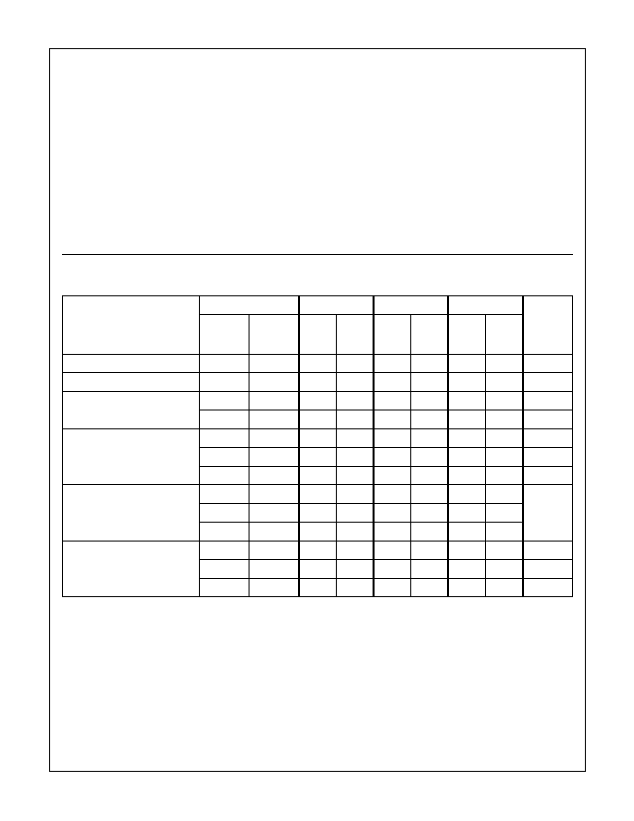
Recommended Operating Conditions TA = -40oC to +85oC. For maximum reliability, operating conditions should be selected so
that operation is always within the following ranges:
TEST CONDITIONS
CDP1802A
CDP1802AC
CDP1802BC
PARAMETER
(NOTE 2)
VCC
VDD
(V)
(V)
MIN MAX
MIN
MAX MIN MAX
UNITS
DC Operating Voltage Range
-
-
4
10.5
4
6.5
4
6.5
V
Input Voltage Range
Maximum Clock Input Rise or
Fall Time
-
-
VSS
VDD
VSS
VDD
VSS
VDD
V
4 to 6.5
4 to 6.5
-
-
-
1
-
1
µs
4 to 10.5 4 to 10.5
-
1
-
-
-
-
µs
Minimum Instruction Time
(Note 3)
5
5
5
-
5
-
3.2
-
µs
5
10
4
-
-
-
-
-
µs
10
10
2.5
-
-
-
-
-
µs
Maximum DMA Transfer Rate
5
5
-
400
-
400
-
667 KBytes/s
5
10
-
500
-
-
-
-
10
10
-
800
-
-
-
-
Maximum Clock Input Frequency,
5
fCL, Load Capacitance
(CL) = 50pF
5
10
5
DC
3.2
DC
3.2
DC
5
MHz
10
DC
4
-
-
-
-
MHz
10
DC
6.4
-
-
-
-
MHz
NOTES:
1. Printed circuit board mount: 57mm x 57mm minimum area x 1.6mm thick G10 epoxy glass, or equivalent.
2. VCC must never exceed VDD.
3. Equals 2 machine cycles - one Fetch and one Execute operation for all instructions except Long Branch and Long Skip, which require 3
machine cycles - one Fetch and two Execute operations.
4. θJA is measured with component mounted on an evaluation board in free air.
3-6
Share Link: 