CDP1871 データシートの表示(PDF) - Intersil
部品番号
コンポーネント説明
メーカー
CDP1871 Datasheet PDF : 10 Pages
| |||
CDP1871A, CDP1871AC
and read by the CPU, at which time the next key pressed in
the scanning order is detected. If the first key remains closed
after the CPU reads the data and resets the DA output, on
the low-to-high transition of TPB, an auxiliary signal (RPT) is
generated and is available to the CPU to indicate an auto-
repeat condition. The RPT output is reset high at the end of
the debounce delay after the depressed key is released.
The DEBOUNCE input provides a terminal connection for an
external user-selected RC circuit to eliminate false detection
of a keydown condition caused by keyboard noise. The oper-
ation of the DEBOUNCE circuit is shown in Figure 2 (Pin
36). When a valid keydown is detected, the on-chip active-
resistor device (RN) is enabled and the external capacitor
(CX) is discharged, providing a key closure debounce time ≅
RNCX. This discharge is sensed by the Schmitt-trigger
inverter, which clocks the DA flip-flop (latching the DA output
low and inhibiting the scan clock). (The DA F/F is reset by
the low-to-high transition of TPB when the CS inputs are
enabled). When a valid key-release is detected RN is dis-
abled and CX begins to charge through the external resistor
(RX), providing a key-release debounce time ≅ RXCX. This
charge time is again sensed by the Schmitt-trigger inverter,
enabling the scan clock to continue on the next high-to-low
transitions of TPB, after the current keycode data is read by
the CPU.
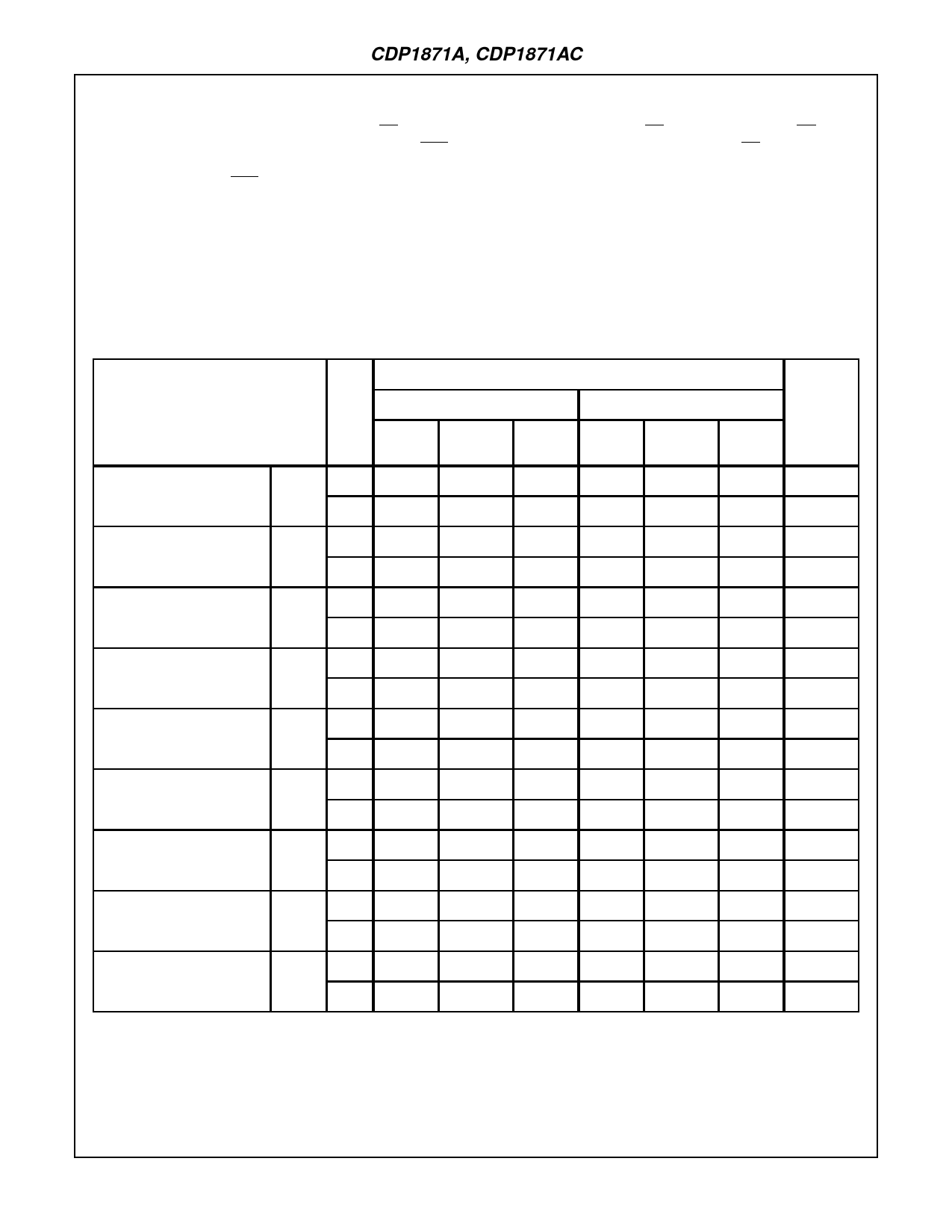
Dynamic Electrical Specifications At TA = -40 to +85oC, VDD ±5%, Unless Otherwise Specified
LIMITS
CDP1871AD, CDP1871AE
CDP1871ACD, CDP1871ACE
PARAMETER
VDD
(NOTE 1)
(V)
MIN
TYP
MAX
(NOTE 1)
MIN
TYP
MAX
UNITS
Clock Cycle Time
tCC
5
-
-
-
-
-
-
Note 2
10
-
-
-
-
-
-
Note 2
Clock Pulse Width High
tCWH
5
100
40
-
100
40
-
ns
10
50
20
-
-
-
-
ns
Data Available Valid Delay
tDAL
5
-
10
-
260
500
-
130
250
-
260
500
ns
-
-
ns
Data Available Invalid Delay
tDAH
5
-
10
-
70
150
-
35
75
-
70
150
ns
-
-
ns
Scan Count Delay
(Non-Repeat)
tCD1
5
-
10
-
850
1900
-
425
950
-
850
1900
ns
-
-
ns
Data Out Valid Delay
tCDV
5
-
10
-
120
250
-
60
125
-
120
250
ns
-
-
ns
Data Out Hold Time
tCDH
5
-
10
-
100
200
-
50
100
-
100
200
ns
-
-
ns
Repeat Valid Delay
tRPL
5
-
10
-
150
400
-
75
200
-
150
400
ns
-
-
ns
Repeat Invalid Delay
tRPH
5
-
10
-
350
700
-
170
350
-
350
700
ns
-
-
ns
NOTES:
1. Typical values are for TA = +25oC and nominal VDD.
2. tCC = tCWH + tCWL
tCWL = tCD1 + KC
k = 0.9ns per pF
c = Keyboard capacitance (pF)
4-73
Share Link: 