CM1220 データシートの表示(PDF) - ON Semiconductor
部品番号
コンポーネント説明
メーカー
CM1220 Datasheet PDF : 6 Pages
| |||
CM1220
Table 4. ELECTRICAL OPERATING CHARACTERISTICS (Note 1)
Symbol
Parameter
Conditions
Min Typ Max
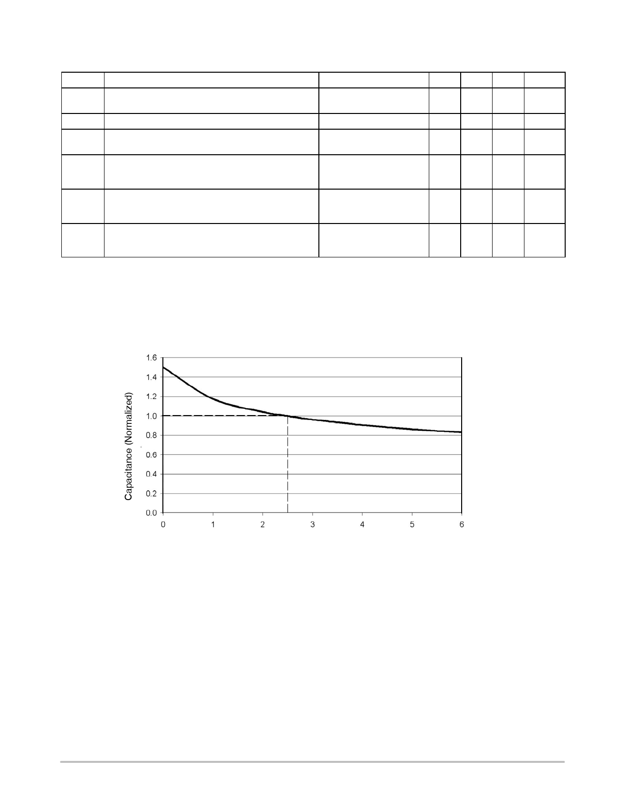
CDIODE Diode (Channel) Capacitance
At 2.5 VDC Reverse Bias,
11
14
17
1 MHz, 30 mVAC
VDIODE
ILEAK
Diode Standoff Voltage
Diode Leakage Current
IDIODE = 10 mA
VIN = +3.3 V
(reverse bias voltage)
6.0
0.1
1
VSIG
Signal Clamp Voltage
Positive Clamp
Negative Clamp
IDIODE = 10 mA
5.6 6.8 9.0
−1.5 −0.8 −0.4
VESD In−system ESD Withstand Voltage
(Note 2)
a) Human Body Model, MIL−STD−883, Method 3015
±30
b) Contact Discharge per IEC 61000−4−2
±15
RDYN Dynamic Resistance
Positive
2.3
Negative
0.9
1. TA = 25 °C unless otherwise specified.
2. ESD applied to input and output pins with respect to GND, one at a time. Unused pins are left open.
Units
pF
V
mA
V
kV
W
PERFORMANCE INFORMATION
Diode Characteristics (nominal conditions unless specified otherwise)
DC Voltage
Figure 1. Insertion Loss vs. Frequency (0 V Bias)
http://onsemi.com
3
Share Link: 