CM1233 гГЗгГЉгВњгВЈгГЉгГИгБЃи°®з§ЇпЉИPDFпЉЙ - ON Semiconductor
йГ®еУБзХ™еПЈ
гВ≥гГ≥гГЭгГЉгГНгГ≥гГИи™ђжШО
гГ°гГЉгВЂгГЉ
CM1233 Datasheet PDF : 13 Pages
| |||
CM1233
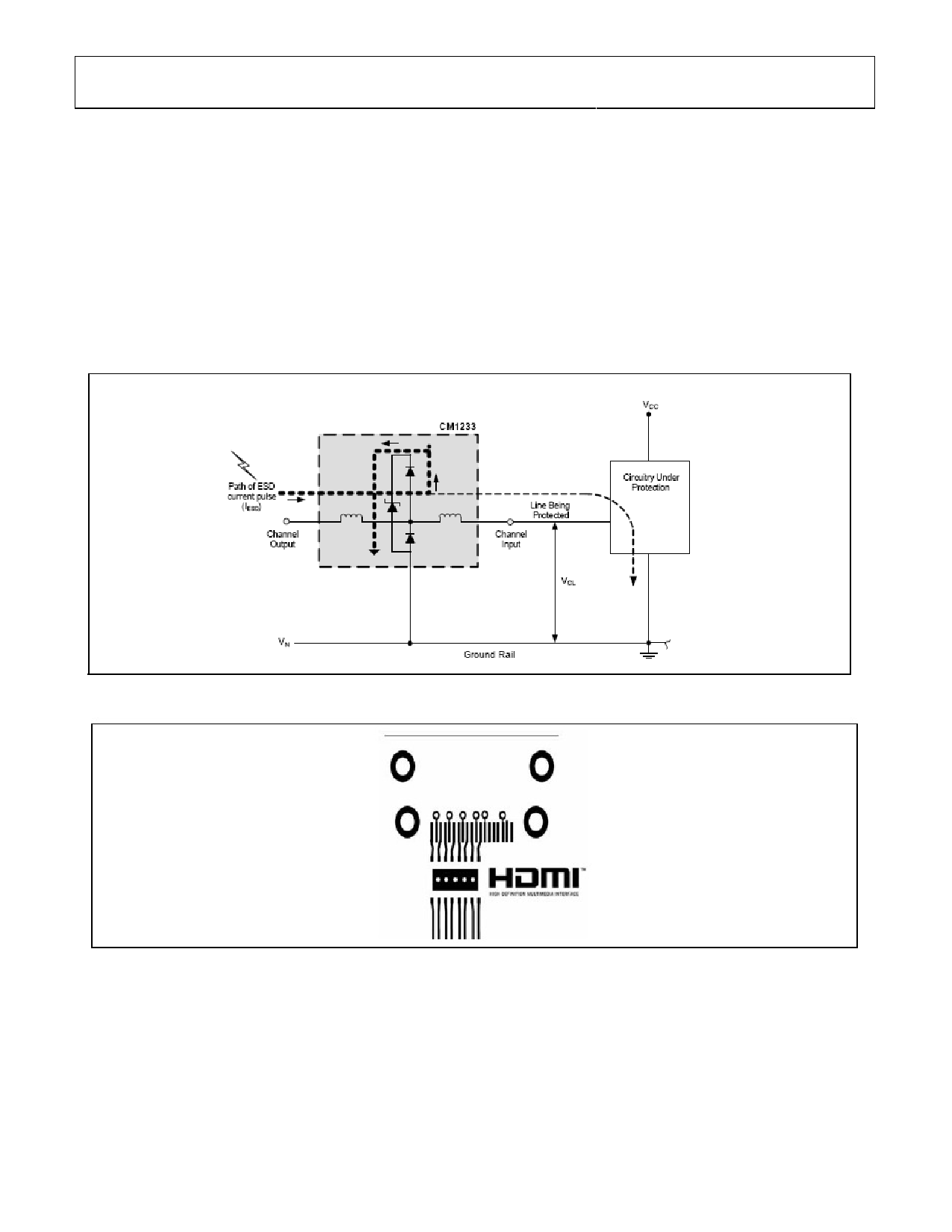
Application Information
CM1233 Application and Guidelines
As a general rule, the CM1233 ESD protection array should be located as close as possible to the point of entry
of expected electrostatic discharges with minimum PCB trace lengths to the ground planes and between the sig-
nal input and the ESD device to minimize stray series inductance.
Figure 8. Application of Positive ESD Pulse Between Input Channel and Ground
Figure 9. Typical PCB Layout
Additional Information
See also California Micro Devices Application Note AP209, вАЬDesign Considerations for ESD Protection,вАЭ in the
Applications section at www.calmicro.com.
Rev. 2 | Page 11 of 13 | www.onsemi.com
Share Link: 