LTC1265I データシートの表示(PDF) - Linear Technology
部品番号
コンポーネント説明
メーカー
LTC1265I Datasheet PDF : 16 Pages
| |||
LTC1265/LTC1265-3.3/LTC1265-5
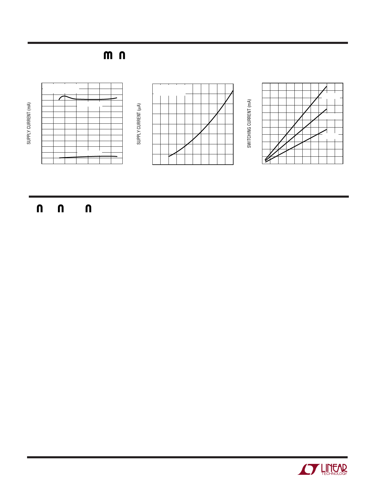
TYPICAL PERFORMANCE CHARACTERISTICS
DC Supply Current
2.1
DOES NOT INCLUDE
GATE CHARGE
1.8
1.5
ACTIVE MODE
1.2
0.9
0.6
0.3
SLEEP MODE
0
0 2 4 6 8 10 12 14
INPUT VOLTAGE (V)
1265 G07
Supply Current in Shutdown
8
SHUTDOWN = 3V
7 TA = 25C
6
5
4
3
2
1
0
3 4 5 6 7 8 9 10 11 12 13
INPUT VOLTAGE (V)
1265 G08
Gate Charge Losses
5.5
5.0
4.5
4.0
3.5
3.0
2.5
2.0
1.5
1.0
VIN = 12V
VIN = 9V
VIN = 6V
0.5
0
0
200 400 600 800
FREQUENCY (kHz)
1000
1265 G09
PIN FUNCTIONS
PWR VIN (Pins 1, 13): Supply for the Power MOSFET and
its Driver. Must decouple this pin properly to ground. Must
always tie Pins 1 and 13 together.
VIN (Pin 2): Main Supply for All the Control Circuitry in the
LTC1265.
LBOUT (Pin 3): Open-Drain Output of the Low-Battery
Comparator. This pin will sink current when Pin 4 (LBIN)
goes below 1.25V. During shutdown, this pin is high
impedance.
LBIN (Pin 4): The (–) Input of the Low-Battery Comparator.
The (+) input is connected to a reference voltage of 1.25V.
CT (Pin 5): External capacitor CT from Pin 5 to ground sets
the switch off time. The operating frequency is dependent
on the input voltage and CT.
ITH (Pin 6): Feedback Amplifier Decoupling Point. The
current comparator threshold is proportional to Pin 6
voltage.
SENSE – (Pin 7): Connect to the (–) input of the current
comparator. For LTC1265-3.3 and LTC1265-5, it also
connects to an internal resistive divider which sets the
output voltage.
SENSE+ (Pin 8): The (+) Pin to the Current Comparator. A
built-in offset between Pins 7 and 8 in conjunction with
RSENSE sets the current trip threshold.
N/C,VFB (Pin 9): For the LTC1265 adjustable version, this
pin serves as the feedback pin from an external resistive
divider used to set the output voltage. On the LTC1265-3.3
and LTC1265-5 versions, this pin is not used.
SHDN (Pin 10): Pulling this pin HIGH keeps the internal
switch off and puts the LTC1265 in micropower shut-
down. Do not float this pin.
SGND (Pin 11): Small-Signal Ground. Must be routed
separately from other grounds to the (–) terminal of COUT.
PGND (Pin 12): Switch Driver Ground. Connects to the
(–) terminal of CIN. Anode of the Schottky diode must be
connected close to this pin.
SW (Pin 14): Drain of the P-Channel MOSFET Switch.
Cathode of the Schottky diode must be connected close to
this pin.
4
Share Link: 