CS61582 データシートの表示(PDF) - Cirrus Logic
部品番号
コンポーネント説明
メーカー
CS61582 Datasheet PDF : 32 Pages
| |||
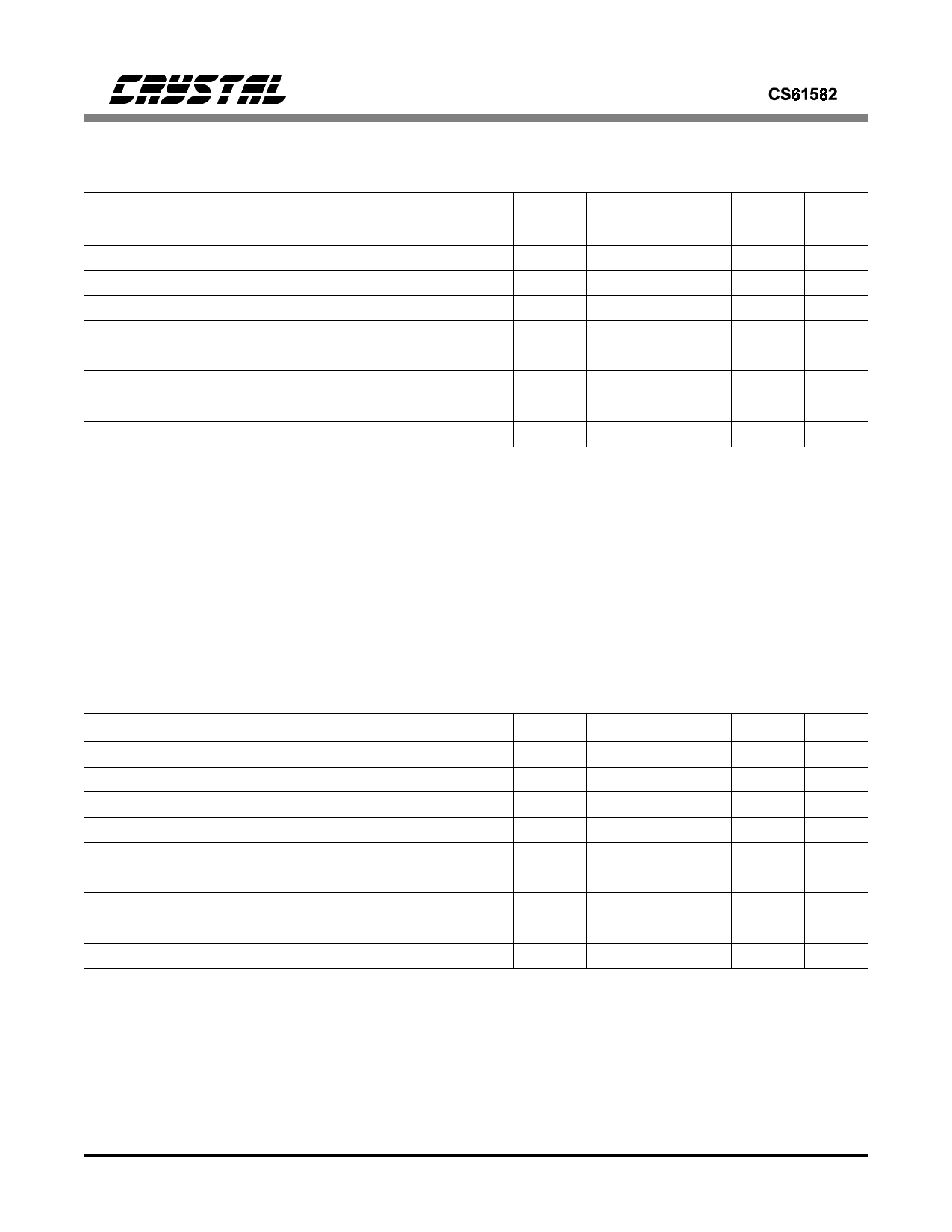
SWITCHING CHARACTERISTICS - T1 CLOCK/DATA (TA = -40 to 85 °C; power supply
pins within ±5% of nominal; Inputs: Logic 0 = 0V, Logic 1 = DV+) (See Figures 1, 2, and 3)
Parameter
Symbol Min
Typ
Max Units
TCLK Frequency
(Note 25) ftclk
-
1.544
-
MHz
TCLK Duty Cycle
tpwh2/tpw2 30
50
70
%
RCLK Duty Cycle
tpwh1/tpw1 45
50
55
%
Rise Time (All Digital Outputs)
(Note 26) tr
-
-
65
ns
Fall Time (All Digital Outputs)
(Note 26) tf
-
-
65
ns
RPOS/RNEG to RCLK Rising Setup Time
tsu1
-
274
-
ns
RCLK Rising to RPOS/RNEG Hold Time
th1
-
274
-
ns
TPOS/TNEG to TCLK Falling Setup Time
tsu2
25
-
-
ns
TCLK Falling to TPOS/TNEG Hold Time
th2
25
-
-
ns
Notes: 25. The maximum burst rate of a gapped TCLK input clock is 8.192 MHz. The maximum gap size
that can be tolerated on TCLK is 28 UIp-p.
26. At max load of 50 pF.
SWITCHING CHARACTERISTICS - E1 CLOCK/DATA (TA = -40 to 85 °C; power supply
pins within ±5% of nominal; Inputs: Logic 0 = 0V, Logic 1 = DV+) (See Figures 1, 2, and 3)
Parameter
TCLK Frequency
TCLK Duty Cycle
RCLK Duty Cycle
Rise Time (All Digital Outputs)
Fall Time (All Digital Outputs)
RPOS/RNEG to RCLK Rising Setup Time
RCLK Rising to RPOS/RNEG Hold Time
TPOS/TNEG to TCLK Falling Setup Time
TCLK Falling to TPOS/TNEG Hold Time
Symbol Min
(Note 25) ftclk
-
tpwh2/tpw2 30
tpwh1/tpw1 45
(Note 26) tr
-
(Note 26) tf
-
tsu1
-
th1
-
tsu2
25
th2
25
Typ
2.048
50
50
-
-
194
194
-
-
Max Units
-
MHz
70
%
55
%
65
ns
65
ns
-
ns
-
ns
-
ns
-
ns
6
DS224PP1
Share Link: 