CS7620 データシートの表示(PDF) - Cirrus Logic
部品番号
コンポーネント説明
メーカー
CS7620 Datasheet PDF : 70 Pages
| |||
CS7620
fixed gain register (16h) should be set and the cali-
bration offset registers (10h - 12h) should be set to
0.
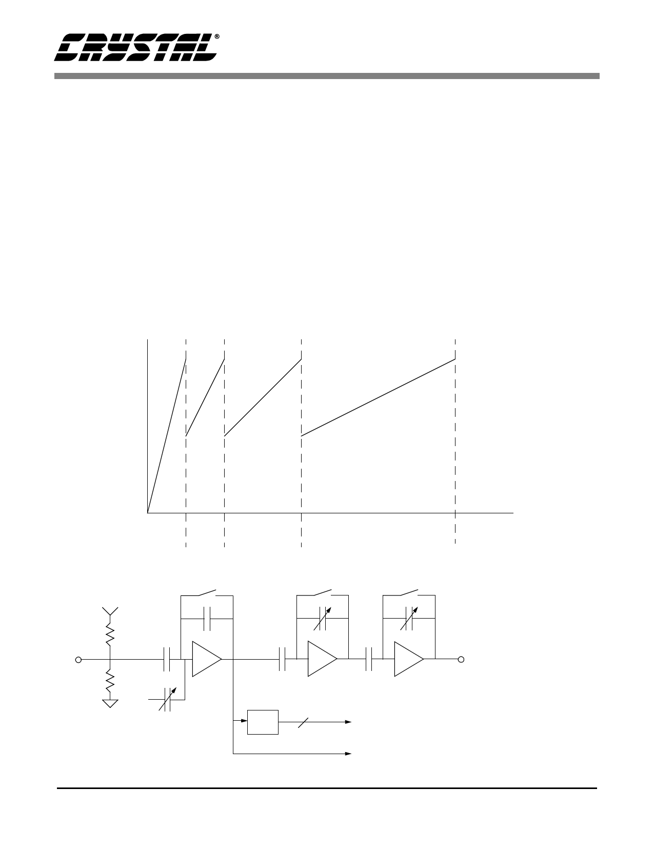
The CDS/VGA circuit is composed of three stages.
The first stage has a fixed gain of 1, and the second
and third stages have variable gain with a combined
gain range of 1 to 8 (0-18 dB). Figure 8 shows a
block diagram of the CDS/VGA circuit. The total
gain is A = (C2/C3)(C4/C5) which is adjusted by
varying C3 and C5. The capacitor Cb on the front
of stage 1 is for black level adjustment and will be
discussed in detail later.
This circuit utilizes a two phase non-overlapping
clock to perform the desired CDS function. The
VOUT (V)
1.07
two phase clock also allows the video signal to be
passed to the output while retaining a positive po-
larity signal. Figure 9 shows a timing diagram of
the two phase clock along with the CCD signal and
output signals of stages one, two and three.
There is an internal mid-scale DC bias level circuit
at the input pin. This allows AC coupling into the
CS7620 with a capacitor and having the input auto-
matically biased to mid-supply without worrying
about external circuitry to perform this task.
3.1 Black Level Adjustment
In order to maintain a constant reference level for
black pixels, a feedback loop is implemented that
0.5
8X 4X
2X
1X
VIN
10
0.13
0.27
0.53
00 01
10
1.07
VIN (V)
11
ADC OUTPUT
Figure 7. Transfer function of VGA circuit (assuming full scale level of 1.07V)
Φ1
Φ2
Φ1
C1
C3
C5
100 KΩ C1
-A1
100 KΩ Cb STAGE 1
VREF
C2
Vo1
C4
-A2
Vo2
STAGE 2
-A3
STAGE 3
VOUT
2
ADC
CONTROLS C3, C5
CONTROLS GAIN ADJUST BLOCK IN DIGITAL
TO AOUT CIRCUITRY
Figure 8. Block diagram of CDS/VGA circuit
DS301PP2
Share Link: 