CS7622-IQ データシートの表示(PDF) - Cirrus Logic
部品番号
コンポーネント説明
メーカー
CS7622-IQ Datasheet PDF : 36 Pages
| |||
CS7622
During fixed gain mode the time constant is a little
different.
For a fixed gain of 1:
τ
=
–-------------1--------------
ln 1
–
n---8-K---
-f-1-u-
For a fixed gain of 2:
τ
=
–-------------1--------------
ln 1
–
n---4-K---
-f-1-u-
For a fixed gain of 4:
τ
=
–-------------1--------------
ln 1
–
n---2-K---
-f-1-u-
For a fixed gain of 8:
τ = –-l--n---(---1----1–-----n---K-----) -f-1-u-
In order to achieve no ringing in the settling use,
-n--
K
≤
1
for offset
range = 1, and
---n----
2K
≤
1
for offset range
= 0.
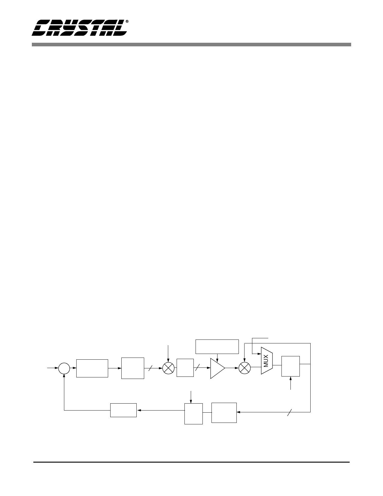
The 9 MSBs of the black level accumulator can be
read or written through a register. If written, the
LSBs are set to zero. The black level is set to “8” in
a 10-bit digital output representation. In a 13-bit
representation, it is set to “64.” The power-up de-
fault value in the accumulator is at mid level.
Also note that the black level adjust loop can be
disabled. In addition, the black level can be pro-
grammed through the serial port.
3.3 Gain Adjust Block
In order to increase the dynamic range of the ADC,
a variable gain, whose value is determined by the
signal level, is applied to each pixel. This allows
for 13 bits of dynamic range and 10 bits of resolu-
tion after accounting for the significance of the
ADC output bits. The gain applied in the analog is
illustrated in the transfer curve in Figure 7. Once
the signal is digitized, the gain adjust block uses the
gain information for a given pixel word and shifts
its bits accordingly. For example, using a full scale
level of 1.0 V, if Vin = 0.3 V, the VGA would
choose a gain of 2X so the ADC input is 0.6 V. The
10-bit output of the ADC (with no black level) is
(0.6/1.0) × 1024 = 614, or “1001100110.” in bina-
ry. The gain adjust block will take this value plus
the bits representing the 2x gain and divide the out-
put by two (shift right by 1). The output of the gain
adjust block is then “0100110011.000.” Note that
the decimal point is virtual, having no existence in
silicon. It is representing the fact that we keep 3 ex-
tra bits of lower significance in the output. In the
same manner, if Vin = 0.75 V, a gain of 1X would
be chosen and the output of the gain adjust block
VIN
Σ
CDS/VGA
ADC
‘64’
BLK LVL LOOP
GAIN REG
10 +
7
+
- CLIP
K
+
FU
DAC
FU = UPDATE FREQUENCY
FP = PIXEL FREQUENCY
BINARY
Z-1
TO
THERM
Figure 10. Black level adjustment loop
FROM SERIAL INTERFACE
Z-1
FP
9
DS322PP1
11
Share Link: 