CS7622 データシートの表示(PDF) - Cirrus Logic
部品番号
コンポーネント説明
メーカー
CS7622 Datasheet PDF : 36 Pages
| |||
CS7622
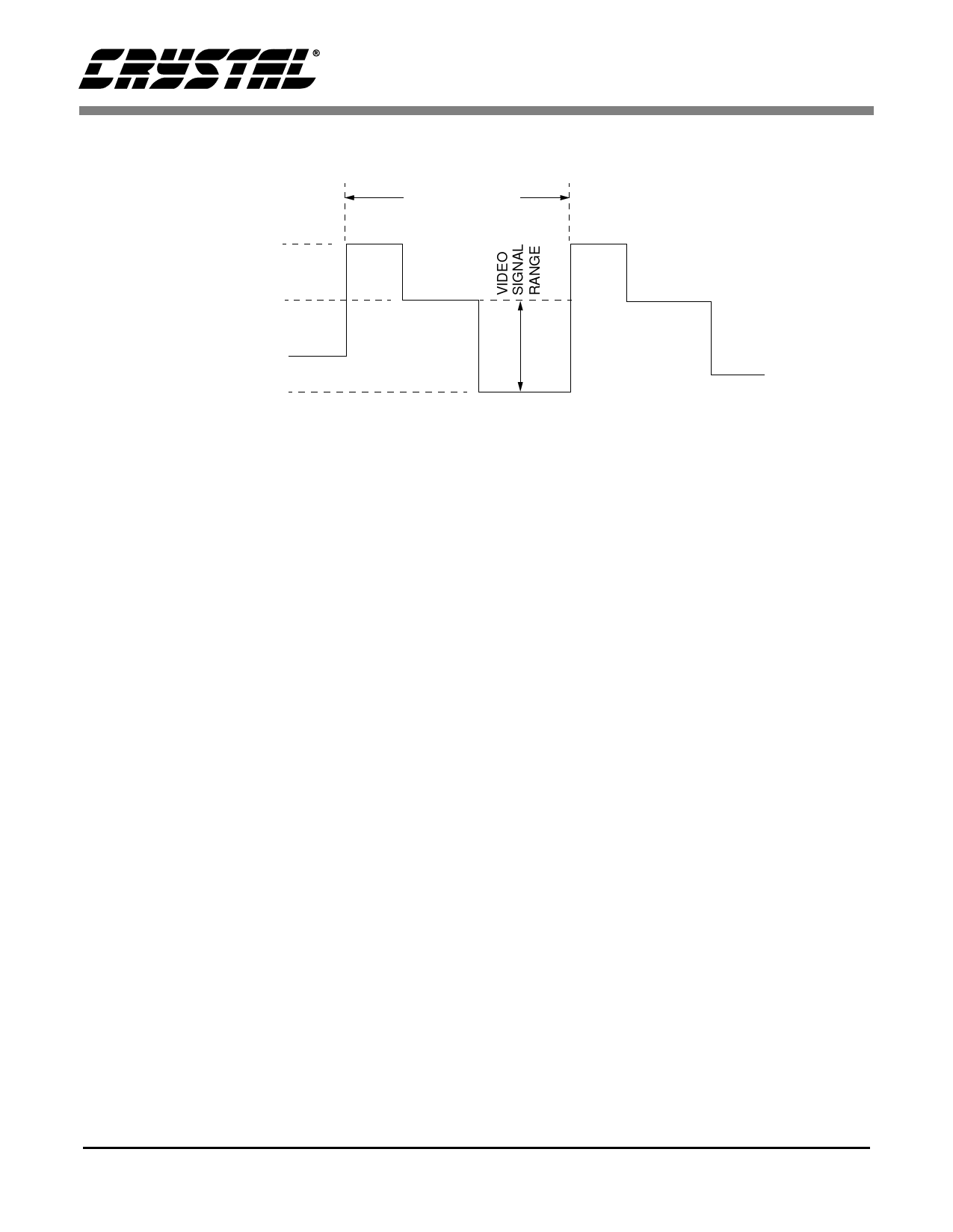
RESET LEVEL
FEED THROUGH
LEVEL
PIXEL PERIOD
DARK
VIDEO LEVEL
MAX. BRIGHTNESS
Figure 6. Idealized CCD output waveform
3.0 OPERATION
3.1 CDS/VGA (correlated double
sampling/variable gain amplification)
An idealized waveform of the CCD output is
shown in Figure 6.
The CCD output contains reset noise, thermal
noise, and 1/f noise generated in the CCD output
circuit. This degrades the S/N ratio and must be
cancelled. Since the noise during the active video
portion of the CCD signal is assumed to be corre-
lated with the noise during the feed through portion
of the signal, this noise can be cancelled by sub-
tracting the feed through level from the video level.
This operation is called correlated double sam-
pling. The active video signal is the difference be-
tween the feed through and video levels. The active
video signal varies according to light conditions. In
order to insure that the full dynamic range of the
ADC is utilized even under low light conditions,
the CCD output is amplified using a VGA. The
gain control is provided by a 2 bit control word
generated by an ADC after stage 1, which has a
gain of 1. Based on the input voltage, a gain of 1x,
2x, 4x, or 8x is subsequently applied to the signal.
The amount of gain is later adjusted in the digital
section. After the VGA, the signal gets digitized by
a 10 bit ADC. The 2 bit ADC output is used in
combination with the 10 bit ADC output to produce
a 13 bit output.
Adding more gain before the ADC does not offer
performance improvement because the noise of the
CCD (after gain is applied to it) begins to dominate
over the quantization noise. Any additional gain
should be done in digital since the performance is
the same as when the ADC output has the addition-
al gain applied.
In order to add more flexibility, the full scale input
range is programmable through register 05h. This
setting will determine what input level maps to the
highest ADC output code. Thus depending on the
saturation level of the particular CCD used in the
system, an appropriate full scale input level can be
chosen in the CS7622. The choices of full scale in-
put level are 300 mV to 1 V in 100 mV increments.
In the remainder of this document, all the figures
and discussions assume a full scale level of 1 V is
used.
The transfer function of the VGA portion of the cir-
cuit is shown in Figure 7 with full scale level = 1 V.
It is assumed that the CDS has already been per-
formed. If desired, the gain switching functionality
can be disabled and forced to a fixed gain of 8x, 4x,
2x, or 1x. This way any dynamic range enhance-
ment is lost and the digital output is only 10 bits. If
8
DS322PP1
Share Link: 