CXA1819 データシートの表示(PDF) - Sony Semiconductor
部品番号
コンポーネント説明
メーカー
CXA1819 Datasheet PDF : 20 Pages
| |||
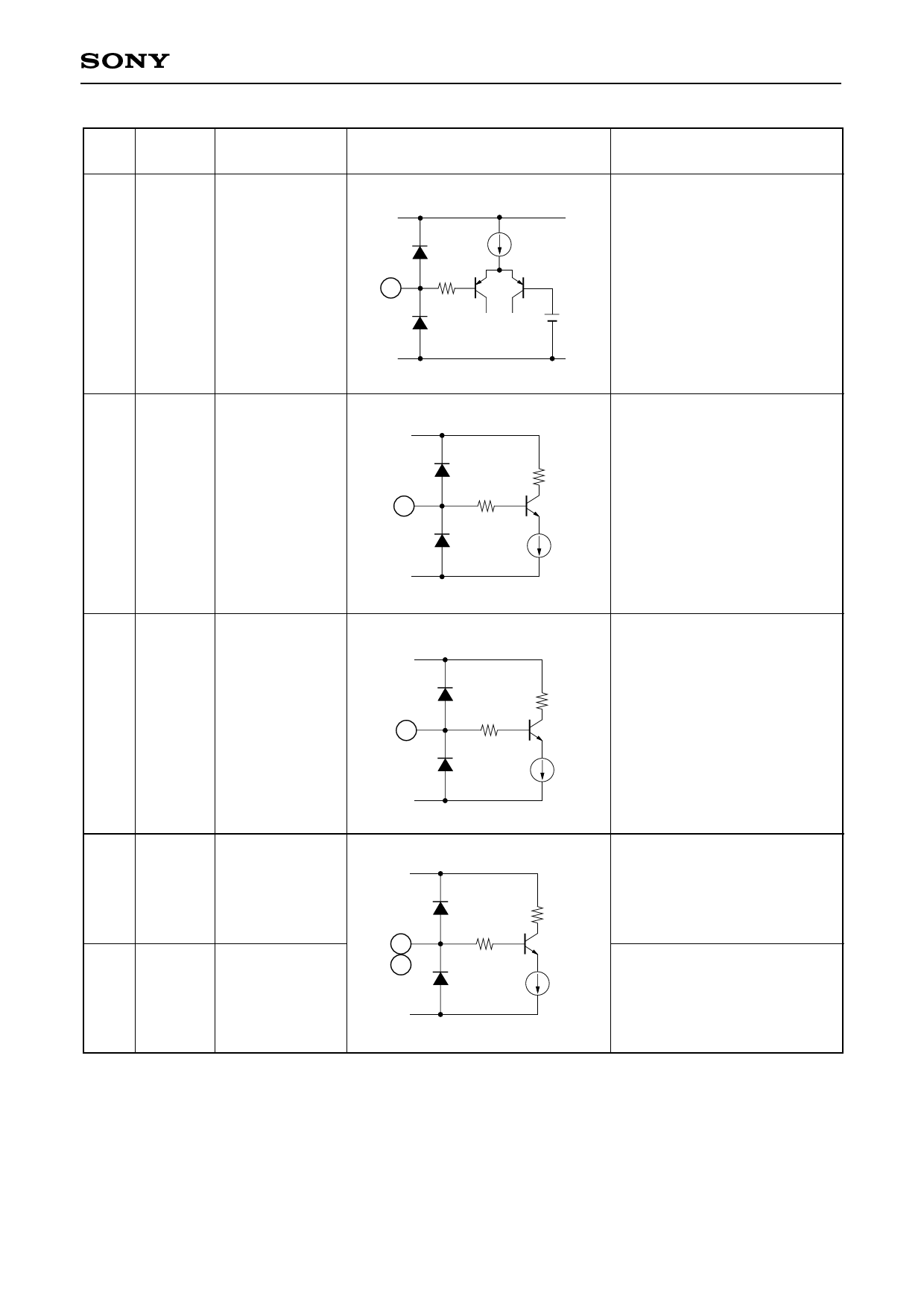
CXA1819Q
Pin
No.
Symbol
Pin voltage
26 PRG
0V∗
Equivalent circuit
Description
VCC1
26
129
GND1
100µA
2.5V
This pin switches black level
and gray level output of the
SID signal. Black level is
output for 0V and gray level is
output for 5V. This pin should
normally be set to 0V.
27 SID BRT
1.6 to 5V∗
1.5k
27
129
SID signal black level control.
50µA
28
RGB
BRT
1.6 to 5V∗
VCC1
28
129
GND1
400
150µA
RGB signal common
brightness control.
Brightness variable range:
5 to 9.8V
29 R BRT
1.6 to 5V∗
30 B BRT
1.6 to 5V∗
VCC1
29
30
129
GND1
Note) ∗ in the Pin voltage indicates external applied voltage.
R signal brightness control.
Brightness variable range
(difference with G signal):
1.5k
–1.0 to +0.7V
B signal brightness control.
50µA Brightness variable range
(difference with G signal):
–1.0 to +0.7V
–7–
Share Link: 