CXA1870 データシートの表示(PDF) - Sony Semiconductor
部品番号
コンポーネント説明
メーカー
CXA1870 Datasheet PDF : 40 Pages
| |||
CXA1870S
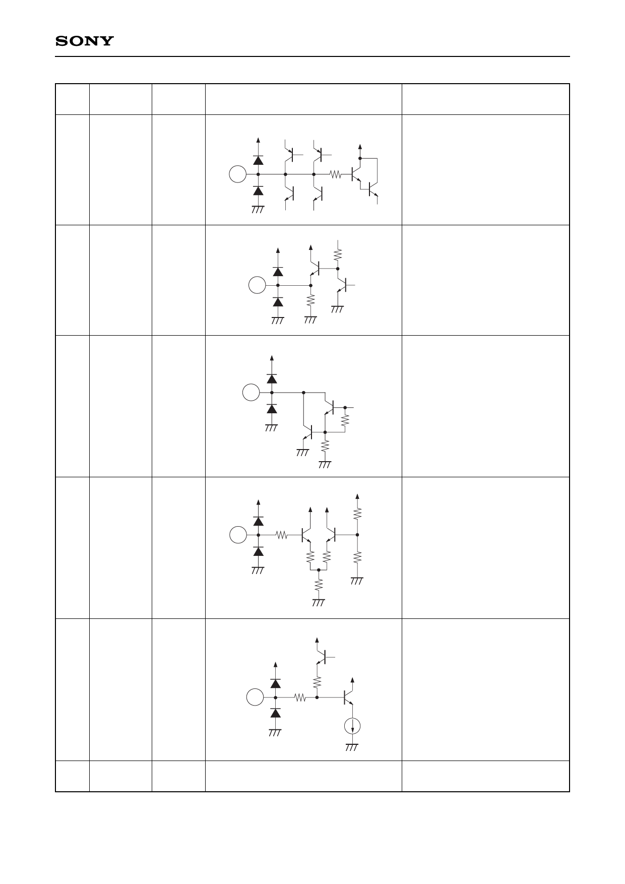
Pin
Pin
Symbol
No.
voltage
27 V LPF
5V
Equivalent circuit
VCC
VCC
27
Description
Connect a capacitor to hold the
AGC voltage which maintains the
V sawtooth wave at a constant
amplitude.
28 V PLS
—
29
HD
—
30
XRAY
—
3.3 V
31
HP
(at no
signal)
VCC
VCC
74k
28
18k
VCC
V pulse output pin. A negative
polarity pulse 3 to 3.5 H width is
output from this pin.
High level: 4.5 V
Low level: 0 V
29
H drive output pin. This pin is
output at the open collector.
20k
20k
VCC
VCC VCC
19k
30
VCC
63k
30k
30k 27k
40k
VCC
VCC
10k
31
VCC
60k
X-ray protection circuit input pin.
When a pulse with a width of 7 V
or more is input, HD output
becomes low and R, G and B
outputs are blanked. This status
is maintained until the power
supply is turned off.
Vilmax = 2.4 V
Vihmin = 3.0 V
H pulse input pin. Inputs a 3 to 5
Vp-p signal via a capacitor.
32 J GND
—
—8—
Jungle system (H/V) GND pin.
Share Link: 