CXA2586M データシートの表示(PDF) - Sony Semiconductor
部品番号
コンポーネント説明
メーカー
CXA2586M Datasheet PDF : 8 Pages
| |||
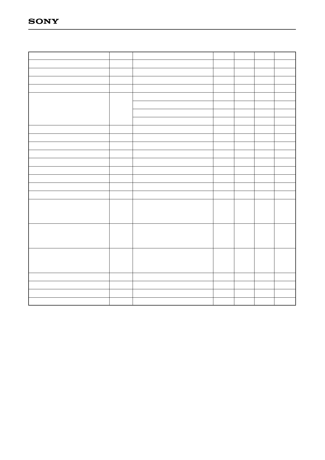
CXA2586M
Electrical and Optical Characteristics
(VCC=5.0 V, VC=2.5 V, Ta=25 °C)
Item
Current consumption
Output offset voltage (A to D)
Output offset voltage (E, F)
Output offset voltage (RF)
Symbol
ICC
Voff
Voff
Voff
Output voltage difference
∆Voff
Sum of output offset voltages
Output voltage (A to D)
Output voltage (E, F)
Output voltage (RF)
Output voltage ratio (E, F/A to D)
Output voltage ratio (RF/A to D)
Maximum output voltage (A to D)
Maximum output voltage (E, F)
Maximum output voltage (RF)
Voffs
Vo
Vo
Vo
VOR
VOR
Vo
Vo
Vo
Frequency response (A to D)
fc
Frequency response (E, F)
fc
Frequency response (RF)
fc
Group delay difference (A to D)
Group delay difference (RF)
Output noise level (A to D)
Output noise level (RF)
∆ Gd
∆ Gd
Vn
Vn
Conditions
In the dark
In the dark, Vc reference
In the dark, Vc reference
In the dark, GND reference
A-B, in the dark
C-D, in the dark
(A+C) – (B+D), in the dark
E-F, in the dark
A+B+C+D, in the dark
λ=650 nm, 780 nm, Po=10 µW
λ=650 nm, 780 nm, Po=10 µW
λ=650 nm, 780 nm, Po=10 µW
λ=650 nm, 780 nm, Po=10 µW
λ=650 nm, 780 nm, Po=10 µW
λ=650 nm, 780 nm, Po=100 µW
λ=650 nm, 780 nm, Po=100 µW
λ=650 nm, 780 nm, Po=100 µW
λ=650 nm, 780 nm
Po=10 µWDC, 4 µWp-p
100 kHz reference, –3 dB
λ=650 nm,780 nm
Po=10 µWDC, 4 µWp-p
100 kHz reference, –3 dB
λ=650 nm, 780 nm
Po=10 µWDC, 4 µWp-p
100 kHz reference, –3 dB
100 kHz to 50 MHz
100 kHz to 50 MHz
f=50 MHz, RBW=30 kHz
f=50 MHz, RBW=30 kHz
Min.
—
–25
–15
1.25
–20
–20
–20
–15
–100
180
312
302
1.71
1.67
3.8
3.8
3.8
70
1
80
—
—
—
—
Typ.
15
0
0
1.4
0
0
0
0
0
246
447
432
1.81
1.76
4.0
4.0
4.0
100
5
105
1
1
–87
–76
Max.
20
25
15
1.55
20
20
20
15
100
312
581
561
1.90
1.84
—
—
—
—
—
—
5
5
–82
–71
Unit
mA
mV
mV
V
mV
mV
mV
mV
mV
mV
mV
mV
—
—
V
V
V
MHz
MHz
MHz
ns
ns
dBm
dBm
Note 1) Output offset voltage: Vc is the reference for A to F, GND for RF.
Note 2) Output voltage: Vc is the reference for A to F, GND for RF. However, the offset voltage is excluded.
Note 3) Output voltage, frequency response, group delay, output noise level: Confirmation of design.
Note 4) Measurement by the optical input: Measurement is made by emitting the light to the center of each
photodiode.
In regard of the frequency response of A to D and RF, the same response can be obtained by emitting
the light to the A to D photodiodes evenly.
—3—
Share Link: 