CXD1261 データシートの表示(PDF) - Sony Semiconductor
部品番号
コンポーネント説明
メーカー
CXD1261 Datasheet PDF : 23 Pages
| |||
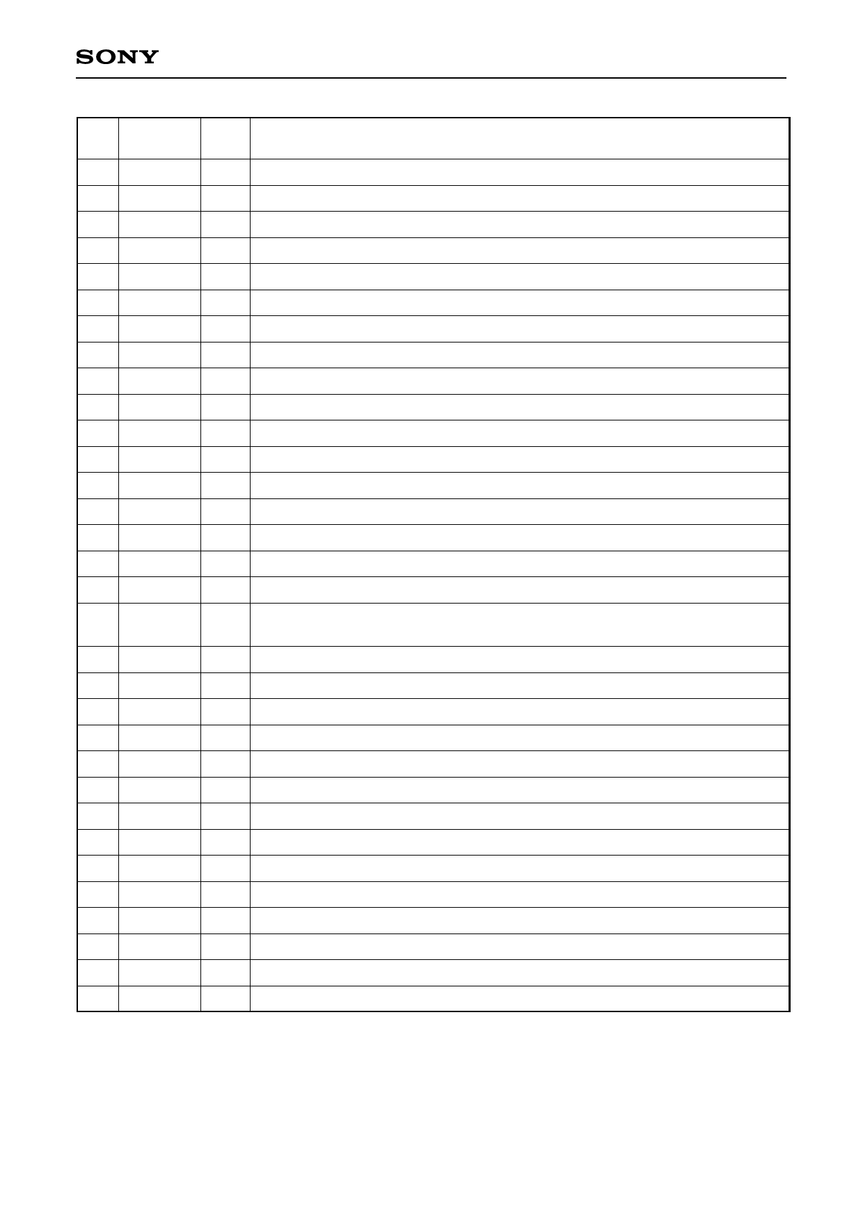
CXD1261AR
Pin
No.
Symbol
33 SHP
34 SHD
35 TST4
36 TST5
37 TST6
38 TST7
39 TST8
40 VSS
41 CLP1
42 CLP2
43 CLP3
44 CLP4
45 PBLK
46 TST9
47 VDD
48 HR
49 VR/FLD
50 HTSG
51 VDD
52 EXT
53 VSS
54 TST10
55 TST11
56 VDD
57 TST12
58 TST13
59 VSS
60 TST14
61 TST15
62 TST16
63 CBLK
64 SYNC
I/O
Description
O Precharge level sample-and-hold pulse
O Data sample-and-hold pulse
O Test output, normally open
O Test output, normally open
O Test output, normally open
O Test output, normally open
O Test output, normally open
— GND
O Clamp pulse
O Clamp pulse
O Clamp pulse
O Clamp pulse
O Blanking cleaning pulse
O Test output, normally open
— Power supply
I H reset pulse
I V reset pulse (FLD output when EXT = low)
I
HTSG input; low: XSG1, 2 on; high: off (valid only when EXT = low)
Fixed to low when EXT = high
— Power supply
I Sync mode switching; low: internal; high: external sync (with pull-down resistor)
— GND
I Test input, normally open (with pull-down resistor)
O Test output, normally open
— Power supply
O Test output, normally open
I Test input, fixed to low
— GND
O Test output, normally open
O Test output, normally open
O Test output, normally open
O Composite blanking pulse
O Composite sync pulse
–4–
Share Link: 