CXL1501 データシートの表示(PDF) - Sony Semiconductor
部品番号
コンポーネント説明
メーカー
CXL1501 Datasheet PDF : 12 Pages
| |||
CXL1501M
Notes)
∗1 Adjust the output amplitude of the inversion and the non-inversion amplifiers in the signal input block to an
equal value, as well as the phase difference to a precise 180°.
Also set the clock and input signal frequency accurately.
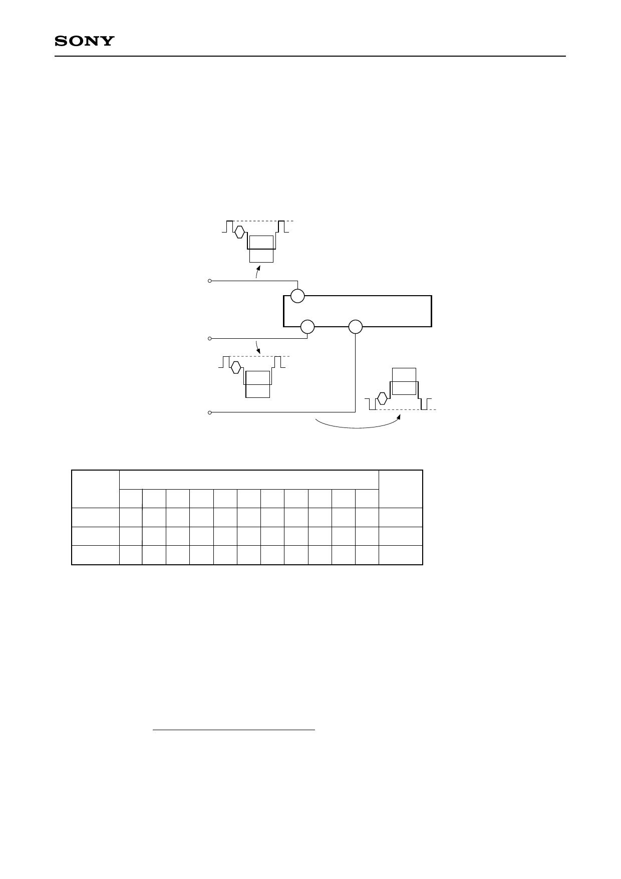
∗2 VIT, VIC and VID are defined as follows:
VIT, VIC and VID are input signal clamp levels. They clamps the Video signal sync tip level. They are the
pin voltages at no-input signal for pins 30, 2 and 5, respectively.
VIT
Input (CCD1)
Input (CCD2)
30
2
VIC
L1501
5
Input (CCD3)
VID
Testing of VIT, VIC and VID is executed with a voltmeter under the following SW conditions:
SW conditions
Test
Item
1 2 3 4 5 6 7 8 9 10 11 point
VIT — b b b a a a — — — — V1
VIC — b b b a a a — — — — V2
VID — b b b a a a — — — — V3
As VIT, VIC and VID differ with each IC, they are to be tested respectively.
∗3 This is the IC supply current value during clock and signal input.
∗4 GLT, GLC and GLD are output gains of TH, Y-YD, and YD pins when a 500mVp-p, 196.678kHz sine wave
is simultaneously fed to CCD1, CCD2, and CCD3 pins respectively.
(Example of calculation)
GLT = 20 log TH pin output voltage [mVp-p] [dB]
500 [mVp-p]
–6–
Share Link: 