CXL1501 データシートの表示(PDF) - Sony Semiconductor
部品番号
コンポーネント説明
メーカー
CXL1501 Datasheet PDF : 12 Pages
| |||
CXL1501M
∗5 GHT, GHC, and GHD are output gains of TH, Y-YD and YD pins when a 150mVp-p, 3.579545MHz sine
wave is simultaneously fed to CCD1, CCD2, and CCD3 pins respectively.
Bias at input (VBIAS1, VBIAS2 and VBIAS3) is tested respectively at VIT – 0.25V, VIC – 0.25V and VID + 0.25V.
(Example of calculation)
GHT = 20 log
TH pin output voltage [mVp-p]
[dB]
150 [mVp-p]
∗6 Indicates the dissipation at 3.579545MHz in relation to 196.678kHz. From the output voltage at TH, Y-YD
and YD pins when a 150mVp-p, 196.678kHz sine wave is simultaneously fed to CCD1, CCD2 and CCD3
pins, and from the output voltage at TH, Y-YD and YD pins when a 150mVp-p, 3.579545MHz sine wave is
simultaneously fed to same, calculation is made according to the following formula. The input block bias for
VBIAS1, VBIAS2 and VBIAS3 is tested at VIT – 0.25V, VIC – 0.25V and VID + 0.25V, respectively.
(Example of calculation)
fT = 20 log TH pin output voltage (3.579545MHz) [mVp-p] [dB]
TH pin output voltage (196.678kHz) [mVp-p]
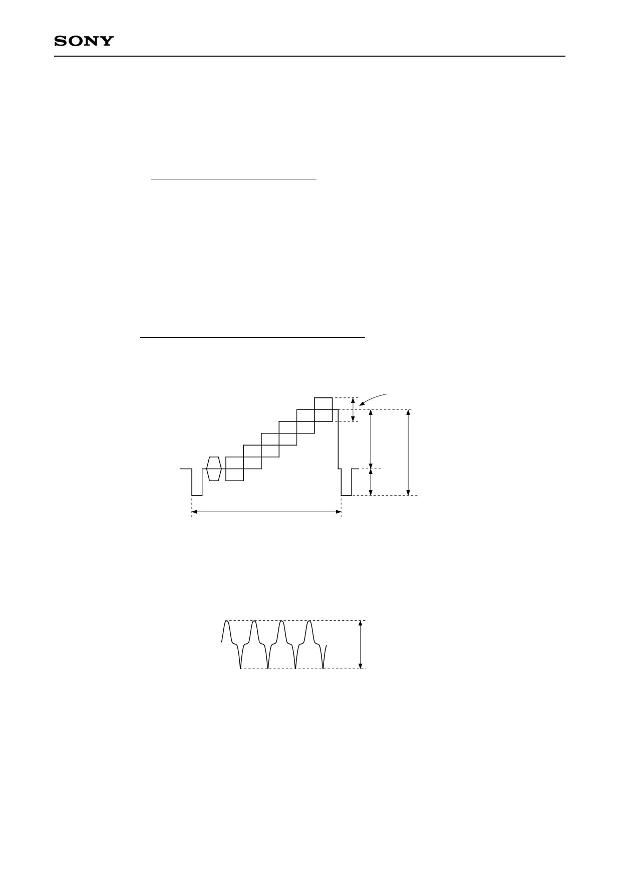
∗7 The differential gain (DG) and the differential phase (DP), when the 5-staircase wave in the following figure
is fed, are tested with a vector scope:
143mV
357mV
500mV
1H 63.56µs
143mV
CCD3 pin input waveform (the input waveform of CCD1 and CCD2 pins is the inverted waveform of the
figure above.)
∗8 The internal clock component to the output signal during no-signal input and the leakage of that high
harmonic component are tested. The input block bias is tested at VITV, VICV, and VID + 0.5V.
Test value [mVp-p]
–7–
Share Link: 