CXL1501 データシートの表示(PDF) - Sony Semiconductor
部品番号
コンポーネント説明
メーカー
CXL1501 Datasheet PDF : 12 Pages
| |||
CXL1501M
∗9 The noise level of output signal at no-input signal is tested with a video noise meter in the Sub Carrier Trap
mode at BPF 100kHz to 4MHz. Vn [Vrms]
The signal component is determined either by testing the output voltage (the same test system as that of
noise level) at input of 357mVp-p, 196.678kHz, or by performing calculation from the values of GLT, GLC,
and GLD in accordance with the following formula. Vs [Vp-p]
(Example of Vs calculation)
GLT
VS-T = 0.357 × 10 20 (VS-T: TH output voltage)
(Example of S/N ratio calculation)
Vn-T (noise component) [Vrms]
SNT = 20 log
[dB]
VS-T (signal component) [Vp-p]
∗10 C-CD is calculated in accordance with the following formula from the Y-YD pin output voltage when a
200mVp-p, 3.579545MHz sine wave is simultaneously fed to CCD1, CCD2 and CCD3 pins and from the Y-
CD pin output voltage when a 200mVp-p, 3.587412MHz sine wave is simultaneously fed to same. The
input block bias is set to VIT – 0.3V, VIC – 0.3V and VID + 0.3V, respectively.
Y-YD pin output voltage (3.587412MHz) [mVp-p]
C-CD = 20 log
[dB]
Y-YD pin output voltage (3.579545MHz) [mVp-p]
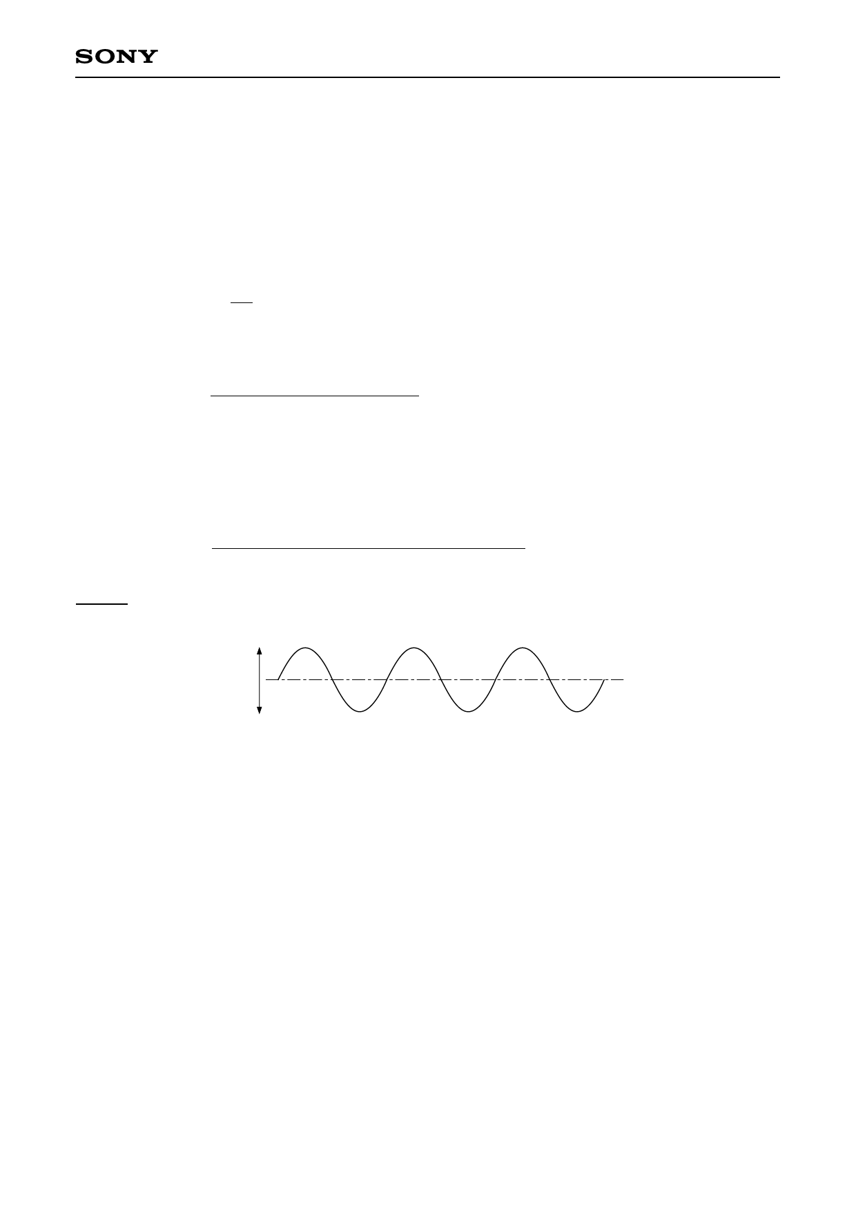
CLOCK
fsc (3.579545MHz) sine wave
0.4Vp-p to 1.0Vp-p
(0.5Vp-p Typ.)
–8–
Share Link: 