CY7B9920(1997) データシートの表示(PDF) - Cypress Semiconductor
部品番号
コンポーネント説明
メーカー
CY7B9920 Datasheet PDF : 7 Pages
| |||
CY7B9910
CY7B9920
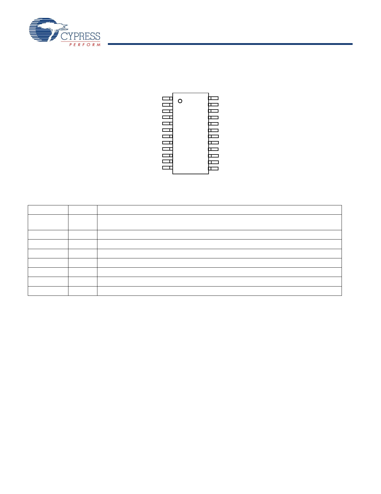
Pin Definitions
Signal
Name
REF
FB
FS[9,10,11]
TEST
Q[0..7]
VCCN
VCCQ
GND
I/O
I
I
I
I
O
PWR
PWR
PWR
Description
Reference frequency input. This input supplies the frequency and timing against which all functional
variation is measured.
PLL feedback input (typically connected to one of the eight outputs).
Three-level frequency range select.
Three-level select. See Test Mode section.
Clock outputs.
Power supply for output drivers.
Power supply for internal circuitry.
Ground.
Maximum Ratings
(Above which the useful life may be impaired. For user guide-
lines, not tested.)
Storage Temperature .................................–65°C to +150°C
Ambient Temperature with
Power Applied.............................................–55°C to +125°C
Supply Voltage to Ground Potential ............... –0.5V to +7.0V
DC Input Voltage............................................ –0.5V to +7.0V
Output Current into Outputs (LOW) ............................. 64 mA
Static Discharge Voltage ........................................... >2001V
(per MIL-STD-883, Method 3015)
Latch-Up Current ..................................................... >200 mA
Operating Range
Range
Commercial
Industrial
Ambient
Temperature
0°C to +70°C
–40°C to +85°C
VCC
5V ± 10%
5V ± 10%
Electrical Characteristics Over the Operating Range
Parameter
VOH
VOL
VIH
VIL
VIHH
VIMM
VILL
IIH
IIL
IIHH
IIMM
IILL
Description
Output HIGH Voltage
Output LOW Voltage
Input HIGH Voltage
(REF and FB inputs only)
Input LOW Voltage
(REF and FB inputs only)
Three-Level Input HIGH
Voltage (Test, FS)[1]
Three-Level Input MID
Voltage (Test, FS)[1]
Three-Level Input LOW
Voltage (Test, FS)[1]
Input HIGH Leakage Current
(REF and FB inputs only)
Input LOW Leakage Current
(REF and FB inputs only)
Input HIGH Current
(Test, FS)
Input MID Current
(Test, FS)
Input LOW Current
(Test, FS)
Test Conditions
VCC = Min., IOH = –16 mA
VCC = Min., IOH =–40 mA
VCC = Min., IOL = 46 mA
VCC = Min., IOL = 46 mA
Min. ≤ VCC ≤ Max.
Min. ≤ VCC ≤ Max.
Min. ≤ VCC ≤ Max.
VCC = Max., VIN = Max.
VCC = Max., VIN = 0.4V
VIN = VCC
VIN = VCC/2
VIN = GND
CY7B9910
Min.
Max.
2.4
0.45
2.0
VCC
–0.5
0.8
CY7B9920
Min.
Max.
VCC – 0.75
VCC –
1.35
–0.5
0.45
VCC
1.35
Unit
V
V
V
V
VCC – 1V VCC
VCC – 1V
VCC
V
VCC/2 – VCC/2 + VCC/2 – VCC/2 + V
500 mV 500 mV 500 mV 500 mV
0.0
1.0
0.0
1.0
V
10
10
µA
–500
–500
µA
200
200 µA
–50
50
–50
50
µA
–200
–200 µA
2
Share Link: 