CY7B9920(1997) データシートの表示(PDF) - Cypress Semiconductor
部品番号
コンポーネント説明
メーカー
CY7B9920 Datasheet PDF : 7 Pages
| |||
CY7B9910
CY7B9920
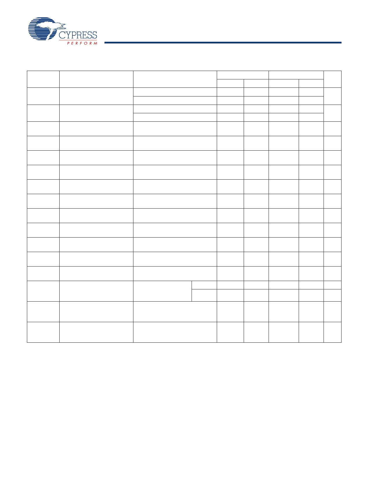
Switching Characteristics Over the Operating Range[7]
CY7B9910–2[8]
Parameter
fNOM
Description
Operating Clock
Frequency in MHz
FS = LOW[9, 10]
FS = MID[9, 10]
FS = HIGH[9, 10, 11]
Min.
15
25
40
Typ.
Max.
30
50
80
tRPWH
tRPWL
tSKEW
tDEV
tPD
tODCV
tORISE
tOFALL
tLOCK
tJR
REF Pulse Width HIGH
REF Pulse Width LOW
Zero Output Skew (All Outputs)[13, 14]
Device-to-Device Skew[14, 15]
Propagation Delay, REF Rise to FB Rise
Output Duty Cycle Variation[16]
Output Rise Time[17, 18]
Output Fall Time[17, 18]
PLL Lock Time[19]
Cycle-to-Cycle Output Jitter Peak to Peak
RMS
5.0
5.0
0.1 0.25
0.75
–0.25 0.0 +0.25
–0.65 0.0 +0.65
0.15 1.0
1.2
0.15 1.0
1.2
0.5
200
25
CY7B9920–2[8]
Min. Typ. Max.
15
30
25
50
40
80[12]
5.0
5.0
0.1 0.25
0.75
–0.25 0.0 +0.25
–0.65 0.0 +0.65
0.5
2.0
2.5
0.5
2.0
2.5
0.5
200
25
Unit
MHz
ns
ns
ns
ns
ns
ns
ns
ns
ms
ps
ps
CY7B9910–5
CY7B9920–5
Parameter
fNOM
Description
Operating Clock
Frequency in MHz
FS = LOW[9, 10]
FS = MID[9, 10]
FS = HIGH[9, 10, 11]
Min.
15
25
40
Typ.
Max.
30
50
80
Min.
15
25
40
Typ.
Max.
30
50
80[12]
Unit
MHz
tRPWH
tRPWL
tSKEW
tDEV
tPD
tODCV
tORISE
tOFALL
tLOCK
tJR
REF Pulse Width HIGH
REF Pulse Width LOW
Zero Output Skew (All Outputs)[13, 14]
Device-to-Device Skew[8, 15]
Propagation Delay, REF Rise to FB Rise
Output Duty Cycle Variation[16]
Output Rise Time[17, 18]
Output Fall Time[17, 18]
PLL Lock Time[19]
Cycle-to-Cycle Output Jitter Peak to Peak[8]
RMS[8]
5.0
5.0
ns
5.0
5.0
ns
0.25 0.5
0.25 0.5
ns
1.0
1.0
ns
–0.5 0.0 +0.5 –0.5 0.0 +0.5 ns
–1.0 0.0 +1.0 –1.0 0.0 +1.0 ns
0.15 1.0
1.5
0.5
2.0
3.0
ns
0.15 1.0
1.5
0.5
2.0
3.0
ns
0.5
0.5 ms
200
200 ps
25
25
ps
Notes:
7. Test measurement levels for the CY7B9910 are TTL levels (1.5V to 1.5V). Test measurement levels for the CY7B9920 are CMOS levels (VCC/2 to VCC/2). Test
conditions assume signal transition times of 2ns or less and output loading as shown in the AC Test Loads and Waveforms unless otherwise specified.
8. Guaranteed by statistical correlation. Tested initially and after any design or process changes that may affect these parameters.
9. For all three-state inputs, HIGH indicates a connection to VCC, LOW indicates a connection to GND, and MID indicates an open connection. Internal termination circuitry
holds an unconnected input to VCC/2.
10. The level to be set on FS is determined by the “normal” operating frequency (fNOM) of the VCO (see Logic Block Diagram). The frequency appearing at the REF and
FB inputs will be fNOM when the output connected to FB is undivided. The frequency of the REF and FB inputs will be fNOM/X when the device is configured for a frequency
multiplication by using external division in the feedback path of value X.
11. When the FS pin is selected HIGH, the REF input must not transition upon power-up until VCC has reached 4.3V.
12. Except as noted, all CY7B9920–2 and –5 timing parameters are specified to 80-MHz with a 30-pF load.
13. tSKEW is defined as the time between the earliest and the latest output transition among all outputs when all are loaded with 50 pF and terminated with 50Ω to
2.06V (CY7B9910) or VCC/2 (CY7B9920).
14. tSKEW is defined as the skew between outputs.
15. tDEV is the output-to-output skew between any two outputs on separate devices operating under the same conditions (VCC, ambient temperature, air flow, etc.).
16. tODCV is the deviation of the output from a 50% duty cycle.
17. Specified with outputs loaded with 30 pF for the CY7B99X0–2 and –5 devices and 50 pF for the CY7B99X0–7 devices. Devices are terminated through 50Ω
to 2.06V (CY7B9910) or VCC/2 (CY7B9920).
18. tORISE and tOFALL measured between 0.8V and 2.0V for the CY7B9910 or 0.8VCC and 0.2VCC for the CY7B9920.
19. tLOCK is the time that is required before synchronization is achieved. This specification is valid only after VCC is stable and within normal operating limits. This parameter is
measured from the application of a new signal or frequency at REF or FB until tPD is within specified limits.
4
Share Link: 