CY7B9910-2SC(1997) データシートの表示(PDF) - Cypress Semiconductor
部品番号
コンポーネント説明
メーカー
CY7B9910-2SC Datasheet PDF : 7 Pages
| |||
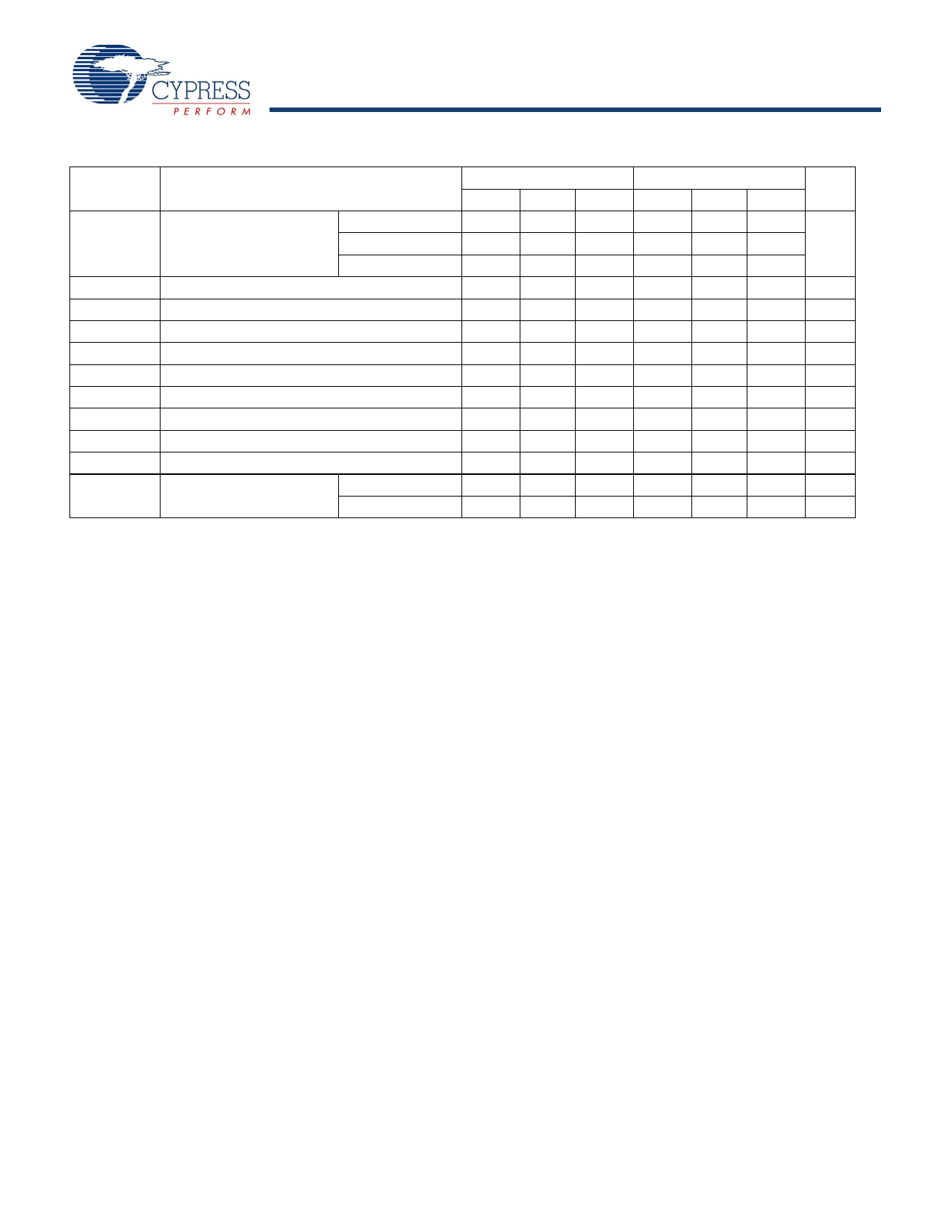
CY7B9910
CY7B9920
SYSTEM
CLOCK
FB
REF
FS
TEST
REF
Q0
Q1
Q2
Q3
Q4
Q5
Q6
Q7
LOAD
Z0
Z0
Z0
Z0
LOAD
LOAD
LOAD
7B9910–9
Figure 1. Zero-Skew and/or Zero-Delay Clock Driver
Operational Mode Descriptions
Figure 1 shows the device configured as a zero-skew clock
buffer. In this mode the 7B9910/9920 can be used as the basis
for a low-skew clock distribution tree. The outputs are aligned
and may each drive a terminated transmission line to an inde-
pendent load. The FB input can be tied to any output and the
operating frequency range is selected with the FS pin. The
low-skew specification, coupled with the ability to drive termi-
nated transmission lines (with impedances as low as 50
ohms), allows efficient printed circuit board design.
Figure 2 shows the CY7B9910/9920 connected in series to
construct a zero-skew clock distribution tree between boards.
Cascaded clock buffers will accumulate low-frequency jitter
because of the non-ideal filtering characteristics of the PLL
filter. It is not recommended that more than two clock buffers
be connected in series.
SYSTEM
CLOCK
REF
FB
REF
FS
Q0
Q1
Q2
Q3
Q4
Q5
Q6
Q7
TEST
LOAD
Z0
LOAD
Z0
LOAD
Z0
FB
REF
FS
Z0
Q0
Q1
Q2
Q3
Q4
Q5
Q6
Q7
TEST
LOAD
LOAD
7B9910–10
Figure 2. Board-to-Board Clock Distribution
6
Share Link: 