CY7C017A データシートの表示(PDF) - Cypress Semiconductor
部品番号
コンポーネント説明
メーカー
CY7C017A Datasheet PDF : 20 Pages
| |||
CY7C006A/CY7C007A
CY7C016A/CY7C017A
Switching Characteristics Over the Operating Range[12] (continued)
Parameter
Description
tWB
R/W HIGH after BUSY (Slave)
tWH
R/W HIGH after BUSY HIGH (Slave)
tBDD[20]
BUSY HIGH to Data Valid
INTERRUPT TIMING[18]
tINS
INT Set Time
tINR
INT Reset Time
SEMAPHORE TIMING
tSOP
tSWRD
tSPS
tSAA
SEM Flag Update Pulse (OE or SEM)
SEM Flag Write to Read Time
SEM Flag Contention Window
SEM Address Access Time
CY7C006A
CY7C007A
CY7C016A
CY7C017A
–12[1]
–15
–20
Min. Max. Min. Max. Min. Max. Unit
0
0
0
ns
11
13
15
ns
12
15
20
ns
12
15
20
ns
12
15
20
ns
10
10
10
ns
5
5
5
ns
5
5
5
ns
12
15
20
ns
Data Retention Mode
The CY7C006A, CY7C007A, CY7C016A, and CY7C017A are
designed with battery backup in mind. Data retention voltage
and supply current are guaranteed over temperature. The
following rules ensure data retention:
1. Chip Enable (CE) must be held HIGH during data retention,
within VCC to VCC – 0.2V.
2. CE must be kept between VCC – 0.2V and 70% of VCC
during the power-up and power-down transitions.
3. The RAM can begin operation >tRC after VCC reaches the
minimum operating voltage (4.5 volts).
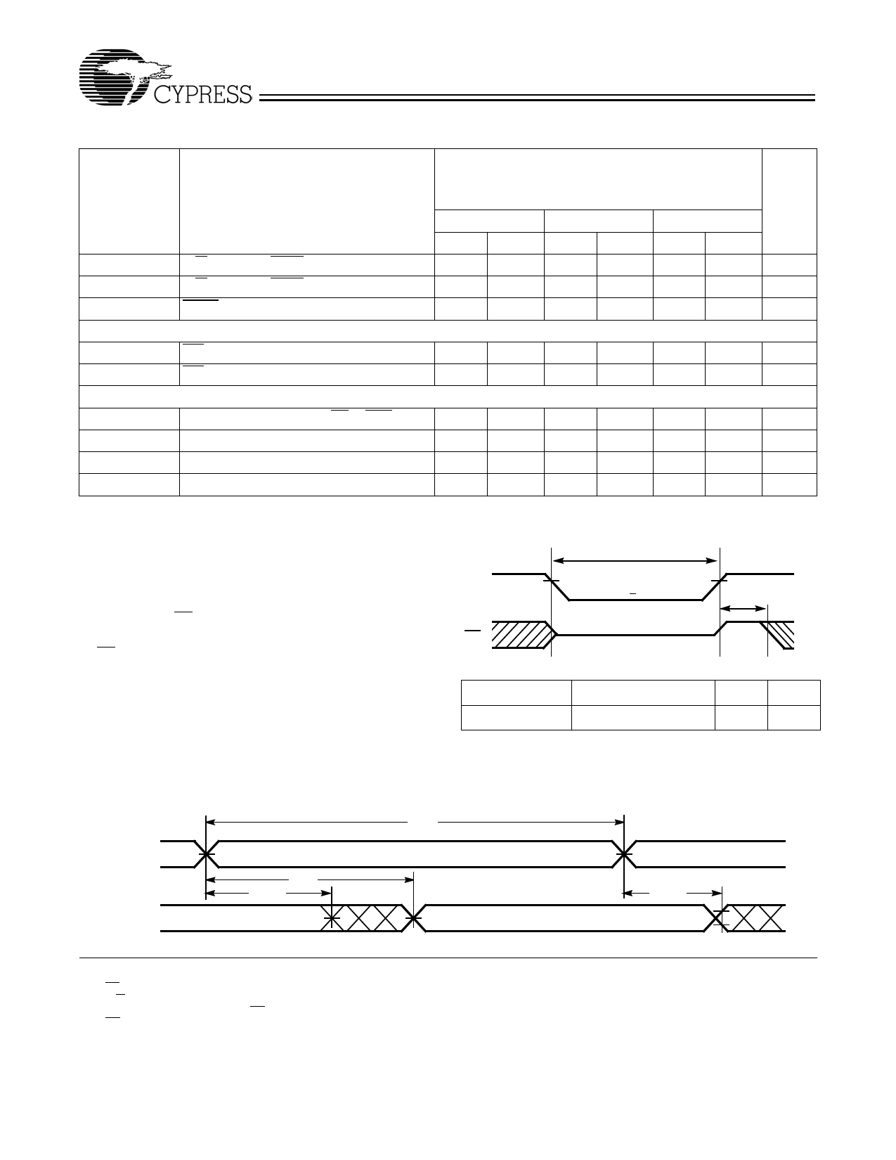
Switching Waveforms
Read Cycle No. 1 (Either Port Address Access)[22, 23, 24]
Timing
VCC
CE
Data Retention Mode
4.5V
VCC > 2.0V
4.5V
VCC to VCC – 0.2V
tRC
VIH
Parameter
ICCDR1
Test Conditions[21]
@ VCCDR = 2V
Max. Unit
1.5 mA
tRC
ADDRESS
DATA OUT
tAA
tOHA
PREVIOUS DATA VALID
DATA VALID
tOHA
Notes:
20. tBDD is a calculated parameter and is the greater of tWDD–tPWE (actual) or tDDD–tSD (actual).
21. CE = VCC, Vin = GND to VCC, TA = 25°C. This parameter is guaranteed but not tested.
22. R/W is HIGH for read cycles.
23. Device is continuously selected CE = VIL. This waveform cannot be used for semaphore reads.
24. OE = VIL.
Document #: 38-06045 Rev. *C
Page 9 of 20
Share Link: 