M59MR032CZC データシートの表示(PDF) - STMicroelectronics
部品番号
コンポーネント説明
メーカー
M59MR032CZC Datasheet PDF : 49 Pages
| |||
M59MR032C, M59MR032D
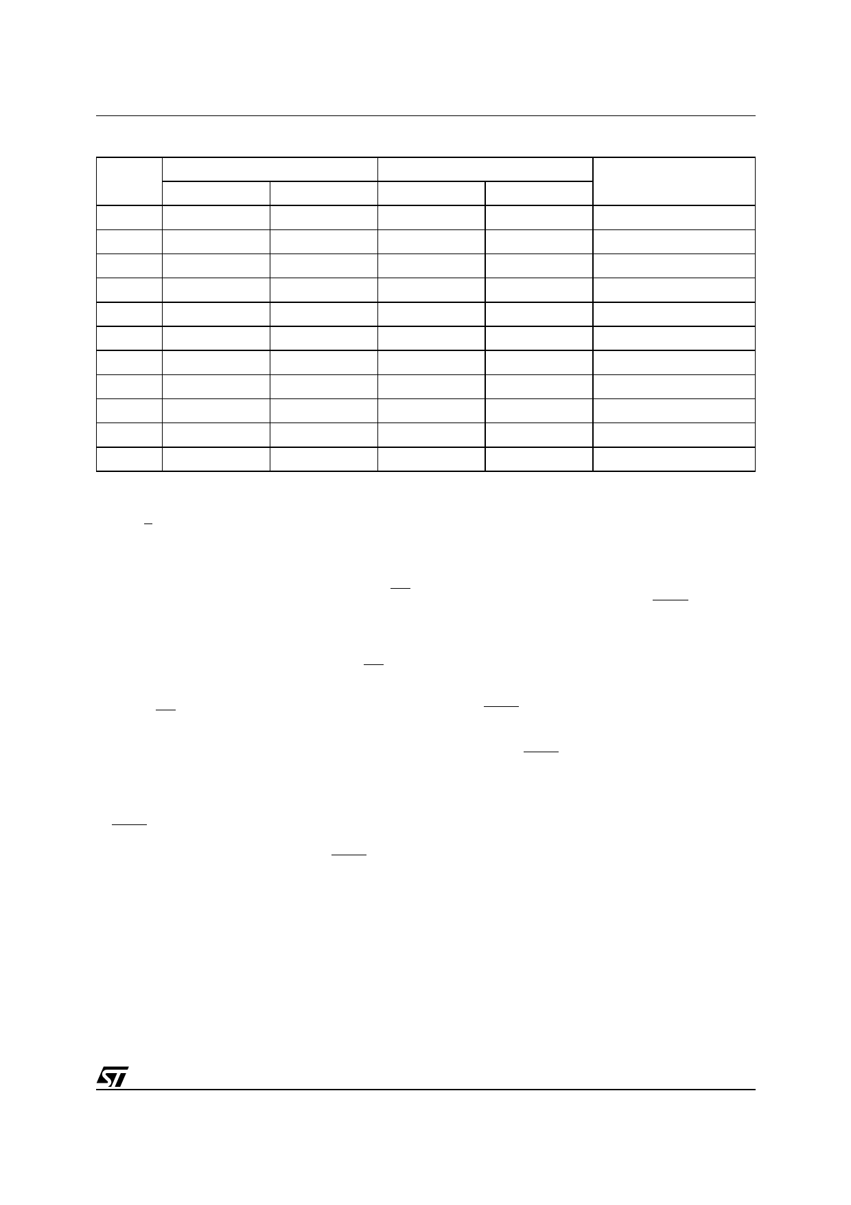
Table 15. Burst Order and Length Configuration
Starting
Address
4 Words
Linear
Interleaved
8 Words
Linear
Interleaved
0
0-1-2-3
0-1-2-3
0-1-2-3-4-5-6-7 0-1-2-3-4-5-6-7
1
1-2-3-0
1-0-3-2
1-2-3-4-5-6-7-0 1-0-3-2-5-4-7-6
2
2-3-0-1
2-3-0-1
2-3-4-5-6-7-0-1 2-3-0-1-6-7-4-5
3
3-0-1-2
3-2-1-0
3-4-5-6-7-0-1-2 3-2-1-0-7-6-5-4
...
7
7-4-5-6
7-6-5-4
7-0-1-2-3-4-5-6 7-6-5-4-3-2-1-0
...
28
29
30
31
Continuous Burst
0-1-2-3-4-5...
1-2-3-4-5-6...
2-3-4-5-6-7...
3-4-5-6-7-8...
7-8-9-10-11...
28-29-30-31-32...
29-30-31-WAIT-32...
30-31-WAIT-WAIT-32...
31-WAIT-WAIT-WAIT-32...
– X-Latency (CR13-CR11). These configuration
bits define the number of clock cycles elapsing
from L going low to valid data available in burst
mode. The correspondence between X-Latency
settings and the sustainable clock frequencies
is given in Table 13 and Figure 5.
– Power-down configuration (CR10). The RP
pin may be configured to give a very low power
consumption when driven low (power-down
state). In power-down the ICC supply current is
reduced to a typical figure of 2µA; if this function
is disabled (default at power-up) the RP pin
causes only a reset of the device and the supply
current is the stand-by value. The recovery time
after a RP pulse is significantly longer (50µs vs.
150ns) when power-down is enabled.
– Data hold configuration (CR9). In
burst
mode this register bit determines if a new data
is output at each clock cycle or every 2 clock cy-
cles.
– Wait configuration (CR8). In burst mode
WAIT indicates whether the data on the output
bus are valid or a wait state must be inserted.
The configuration bit determines if WAIT will be
asserted one clock cycle before the wait state or
during the wait state (see Figure 10).
– Burst order configuration (CR7). See Table
15 for burst order and length.
– Clock configuration (CR6). In burst mode de-
termines if address is latched and data is output
on the rising or falling edge of the clock.
– Burst length (CR2-CR0). In burst mode deter-
mines the number of words output by the mem-
ory. It is possible to have 4 words, 8 words or a
continuous burst mode, in which all the words in
bank A or bank B are read sequentially. In con-
tinuous burst mode the burst sequence is inter-
rupted at the end of each of the two banks or
when a suspended block is reached. In continu-
ous burst mode it may happen that the memory
will stop the data output flow for a few clock cy-
cles; this event is signaled by WAIT going low
until the output flow is resumed. The initial ad-
dress determines if the output delay will occur
as well as its duration. If the starting address is
aligned to a four word boundary no wait states
will be needed. If the starting address is shifted
by 1,2 or 3 positions from the four word bound-
ary, WAIT will be asserted for 1,2 or 3 clock cy-
cles (2,4, 6 cycles if CR9 is set at “1”) when the
burst sequence is crossing the first 32 word
boundary. WAIT will be asserted only once dur-
ing a continuous burst access. See also Table
15.
Enter Bypass Mode (EBY) Instruction. This in-
struction uses the two Coded cycles followed by
one write cycle giving the command 20h to ad-
dress 555h for mode set-up. Once in Bypass
mode, the device will accept the Exit Bypass
(XBY) and Program or Double Word Program in
Bypass mode (PGBY, DPGBY) commands. The
Bypass mode allows to reduce the overall pro-
gramming time when large memory arrays need to
be programmed.
Exit Bypass Mode (XBY) Instruction. This in-
struction uses two write cycles. The first inputs to
the memory the command 90h and the second in-
puts the Exit Bypass mode confirm (00h). After the
XBY instruction, the device resets to Read Memo-
ry Array mode.
15/49
Share Link: 