M59MR032C100ZC6T データシートの表示(PDF) - STMicroelectronics
部品番号
コンポーネント説明
メーカー
M59MR032C100ZC6T
STMicroelectronics

M59MR032C100ZC6T Datasheet PDF : 49 Pages
| |||
M59MR032C, M59MR032D
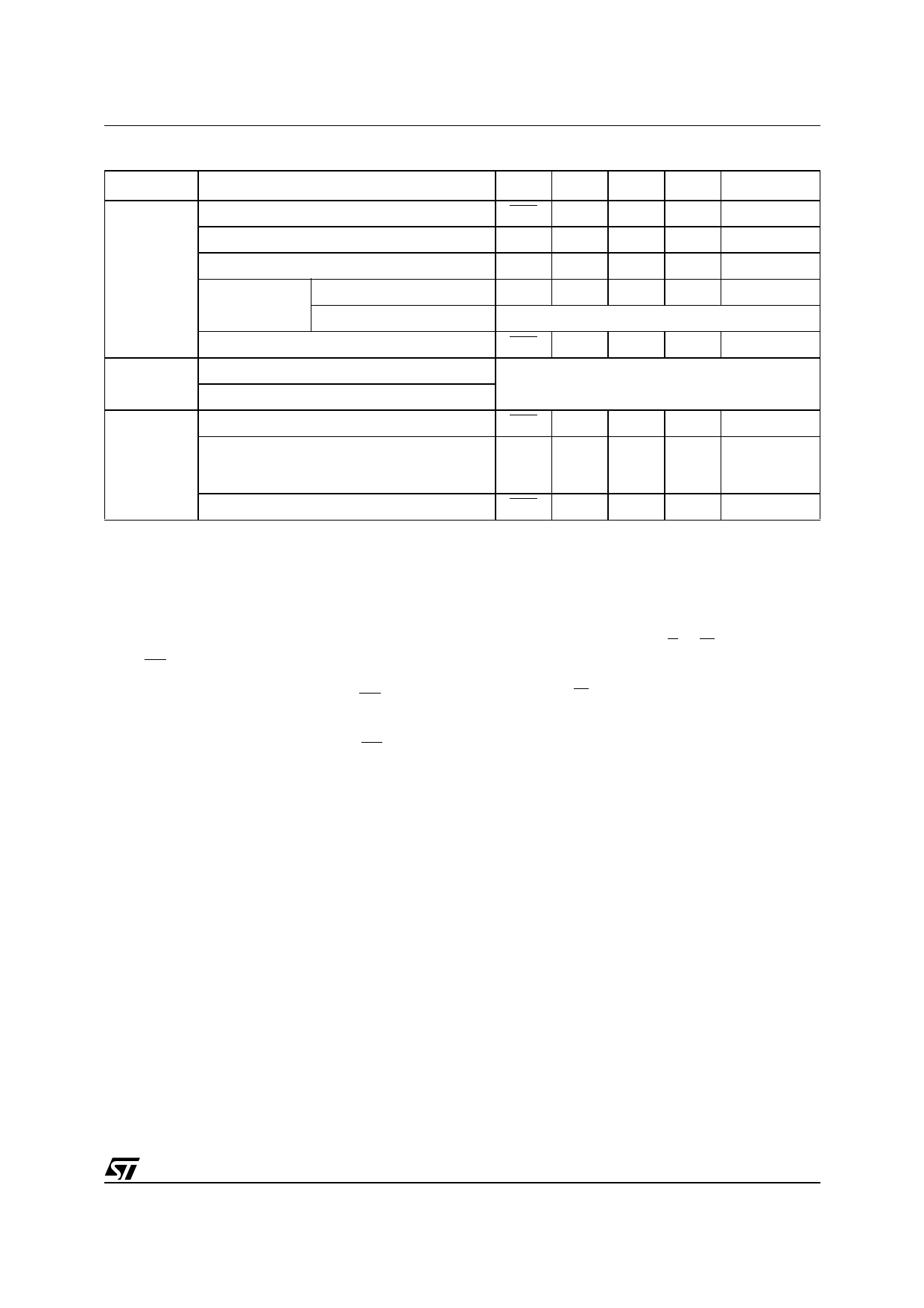
Table 18. Status Register Bits (1)
Status
DQ7 (2) DQ6 DQ5 DQ3
DQ2 (2)
Program
DQ7 Toggle 0
N/A
1
Block Erase Timeout
0 Toggle 0
0
N/A
In Progress
Block/Chip Erase
Erase Suspend Erase Suspended Block
Mode
Non Erase Suspended Block
0 Toggle 0
1
N/A
1
1
0
N/A
Toggle
Automatic return to reading array data
Programming during Erase Suspend
DQ7 Toggle 0
N/A
1
Successfully/ Word Program
Completed Block/Chip Erase
Automatic return to reading array data
Word Program
DQ7 Toggle 1
N/A
1
Exceeded
Time Limit
Block/Chip Erase
0 Toggle 1
Toggle is
1 failed, block is
addressed
Program in Suspend
DQ7 Toggle 1
N/A
1
Note: 1. Status Register bits do not consider BINV.
2. DQ7 and DQ2 require a valid address when reading status information.
POWER CONSUMPTION
Power-down
The memory provides Reset/Power-down control
input RP. The Power-down function can be acti-
vated only if the relevant Configuration Register bit
is set to ’1’. In this case, when the RP signal is
pulled at VSS the supply current drops to typically
ICC2 (see Table 28), the memory is deselected and
the outputs are in high impedance.If RP is pulled
to VSS during a Program or Erase operation, this
operation is aborted in tPLQ7V and the memory
content is no longer valid (see Reset/Power-down
input description).
Power-up
The memory Command Interface is reset on Pow-
er-up to Read Array. Either E or W must be tied to
VIH during Power-up to allow maximum security
and the possibility to write a command on the first
rising edge of W. At Power-up the device is config-
ured as:
– page mode: (CR15 = 1)
– power-down disabled: (CR10 = 0)
– BINV disabled: (CR14 = 0)
and all blocks are protected and unlocked.
Supply Rails
Normal precautions must be taken for supply volt-
age decoupling; each device in a system should
have the VDD rails decoupled with a 0.1µF capac-
itor close to the VDD, VDDQ and VSS pins. The PCB
trace widths should be sufficient to carry the re-
quired VDD program and erase currents.
21/49
Share Link: