CY7C04312BV データシートの表示(PDF) - Cypress Semiconductor
部品番号
コンポーネント説明
メーカー
CY7C04312BV Datasheet PDF : 37 Pages
| |||
CY7C0430BV
CY7C04312BV
CY7C04314BV
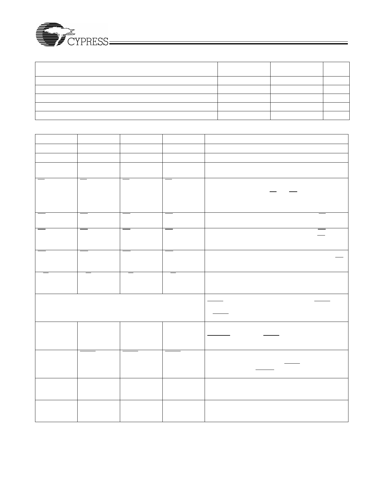
Selection Guide
fMAX2
Max Access Time (Clock to Data)
Max Operating Current ICC
Max Standby Current for ISB1 (All ports TTL Level)
Max Standby Current for ISB3 (All ports CMOS Level)
CY7C04312BV
-133
133[1]
4.2
750
200
15
CY7C04312BV
-100
100
5.0
600
150
15
Unit
MHz
ns
mA
mA
mA
Pin Definitions
Port 1
Port 2
Port 3
Port 4
Description
A0P1–A15P1
I/O0P1–I/O17P1
CLKP1
LBP1
A0P2–A15P2
I/O0P2–I/O17P2
CLKP2
LBP2
A0P3–A15P3
I/O0P3–I/O17P3
CLKP3
LBP3
A0P4–A15P4
I/O0P4–I/O17P4
CLKP4
LBP4
Address Input/Output.
Data Bus Input/Output.
Clock Input. This input can be free running or strobed.
Maximum clock input rate is fMAX.
Lower Byte Select Input. Asserting this signal LOW
enables read and write operations to the lower byte. For
read operations both the LB and OE signals must be
asserted to drive output data on the lower byte of the data
pins.
UBP1
UBP2
UBP3
UBP4
Upper Byte Select Input. Same function as LB, but to
the upper byte.
CE0P1,CE1P1
OEP1
CE0P2,CE1P2
OEP2
CE0P3,CE1P3
OEP3
CE0P4,CE1P4
OEP4
Chip Enable Input. To select any port, both CE0 AND
CE1 must be asserted to their active states (CE0 ≤ VIL
and CE1 ≥ VIH).
Output Enable Input. This signal must be asserted LOW
to enable the I/O data lines during read operations. OE
is asynchronous input.
R/WP1
R/WP2
R/WP3
R/WP4
Read/Write Enable Input. This signal is asserted LOW
to write to the dual port memory array. For read opera-
tions, assert this pin HIGH.
MRST
CNTRSTP1[6]
MKLDP1[6]
CNTLDP1[6]
CNTINCP1[6]
CNTRSTP2[6]
MKLDP2[6]
CNTLDP2[6]
CNTINCP2[6]
CNTRSTP3[6]
MKLDP3[6]
CNTLDP3[6]
CNTINCP3[6]
CNTRSTP4[6]
MKLDP4[6]
CNTLDP4[6]
CNTINCP4[6]
Master Reset Input. This is one signal for All Ports.
MRST is an asynchronous input. Asserting MRST LOW
performs all of the reset functions as described in the text.
A MRST operation is required at power-up.
Counter Reset Input. Asserting this signal LOW resets
the burst address counter of its respective port to zero.
CNTRST is second to MRST in priority with respect to
counter and mask register operations.
Mask Register Load Input. Asserting this signal LOW
loads the mask register with the external address
available on the address lines. MKLD operation has
higher priority over CNTLD operation.
Counter Load Input. Asserting this signal LOW loads
the burst counter with the external address present on
the address pins.
Counter Increment Input. Asserting this signal LOW
increments the burst address counter of its respective
port on each rising edge of CLK.
Document #: 38-06027 Rev. *A
Page 6 of 37
Share Link: 