CY7C0430CV データシートの表示(PDF) - Cypress Semiconductor
部品番号
コンポーネント説明
メーカー
CY7C0430CV Datasheet PDF : 37 Pages
| |||
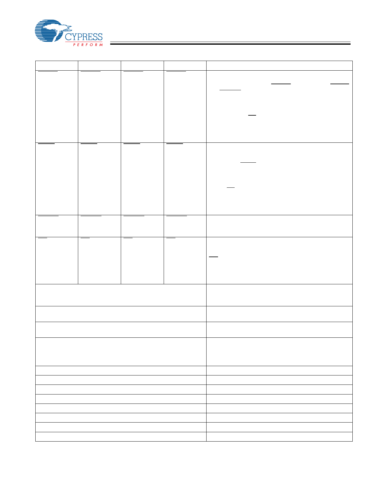
Pin Definitions (continued)
Port 1
CNTRDP1
Port 2
CNTRDP2
Port 3
CNTRDP3
MKRDP1
MKRDP2
MKRDP3
CNTINTP1
CNTINTP2
CNTINTP3
INTP1
INTP2
INTP3
TMS
TCK
TDI
TDO
CLKBIST
GND
VSS
VDD
VSS1
VDD1
VSS2
VDD2
Port 4
CNTRDP4
MKRDP4
CNTINTP4
INTP4
CY7C0430BV
CY7C0430CV
Description
Counter Readback Input. When asserted LOW, the
internal address value of the counter will be read back on
the address lines. During CNTRD operation, both CNTLD
and CNTINC must be HIGH. Counter readback operation
has higher priority over mask register readback operation.
Counter readback operation is independent of port chip
enables. If address readback operation occurs with chip
enables active (CE0 = LOW, CE1 = HIGH), the data lines
(I/Os) will be three-stated. The readback timing will be
valid after one no-operation cycle plus tCD2 from the rising
edge of the next cycle.
Mask Register Readback Input. When asserted LOW,
the value of the mask register will be readback on address
lines. During mask register readback operation, all
counter and MKLD inputs must be HIGH (see Counter
and Mask Register Operations truth table). Mask register
readback operation is independent of port chip enables.
If address readback operation occurs with chip enables
active (CE0 = LOW, CE1 = HIGH), the data lines (I/Os) will
be three-stated. The readback will be valid after one
no-operation cycle plus tCD2 from the rising edge of the
next cycle.
Counter Interrupt Flag Output. Flag is asserted LOW
for one clock cycle when the counter wraps around to
location zero.
Interrupt Flag Output. Interrupt permits communications
between all four ports. The upper four memory locations
can be used for message passing. Example of operation:
INTP4 is asserted LOW when another port writes to the
mailbox location of Port 4. Flag is cleared when Port 4
reads the contents of its mailbox. The same operation is
applicable to ports 1, 2, and 3.
JTAG Test Mode Select Input. It controls the advance of
JTAG TAP state machine. State machine transitions occur
on the rising edge of TCK.
JTAG Test Clock Input. This can be CLK of any port or
an external clock connected to the JTAG TAP.
JTAG Test Data Input. This is the only data input. TDI
inputs will shift data serially in to the selected register.
JTAG Test Data Output. This is the only data output.
TDO transitions occur on the falling edge of TCK. TDO
normally three-stated except when captured data is
shifted out of the JTAG TAP.
BIST Clock Input.
Thermal Ground for Heat Dissipation.
Ground Input.
Power Input.
Address Lines Ground Input.
Address Lines Power Input.
Data Lines Ground Input.
Data Lines Power Input.
Document #: 38-06027 Rev. *B
Page 7 of 37
Share Link: 