CY7C1021D(2009) データシートの表示(PDF) - Cypress Semiconductor
部品番号
コンポーネント説明
メーカー
CY7C1021D Datasheet PDF : 11 Pages
| |||
CY7C1021D
1-Mbit (64K x 16) Static RAM
Features
■ Temperature Ranges:
❐ Industrial: –40°C to 85°C
❐ Automotive-A: –40°C to 85°C
❐ Automotive-E: –40°C to 125°C
■ Pin and Function Compatible with CY7C1021B
■ High Speed
❐ tAA = 10 ns (Industrial)
■ Low Active Power
❐ ICC = 80 mA at 10 ns
■ Low CMOS Standby Power
❐ ISB2 = 3 mA
■ 2.0V Data Retention
■ Automatic Power Down when Deselected
■ CMOS for Optimum Speed and Power
■ Independent Control of Upper and Lower Bits
■ Available in Pb-free 44-Pin 400-Mil Wide Molded SOJ and
44-Pin TSOP II Packages
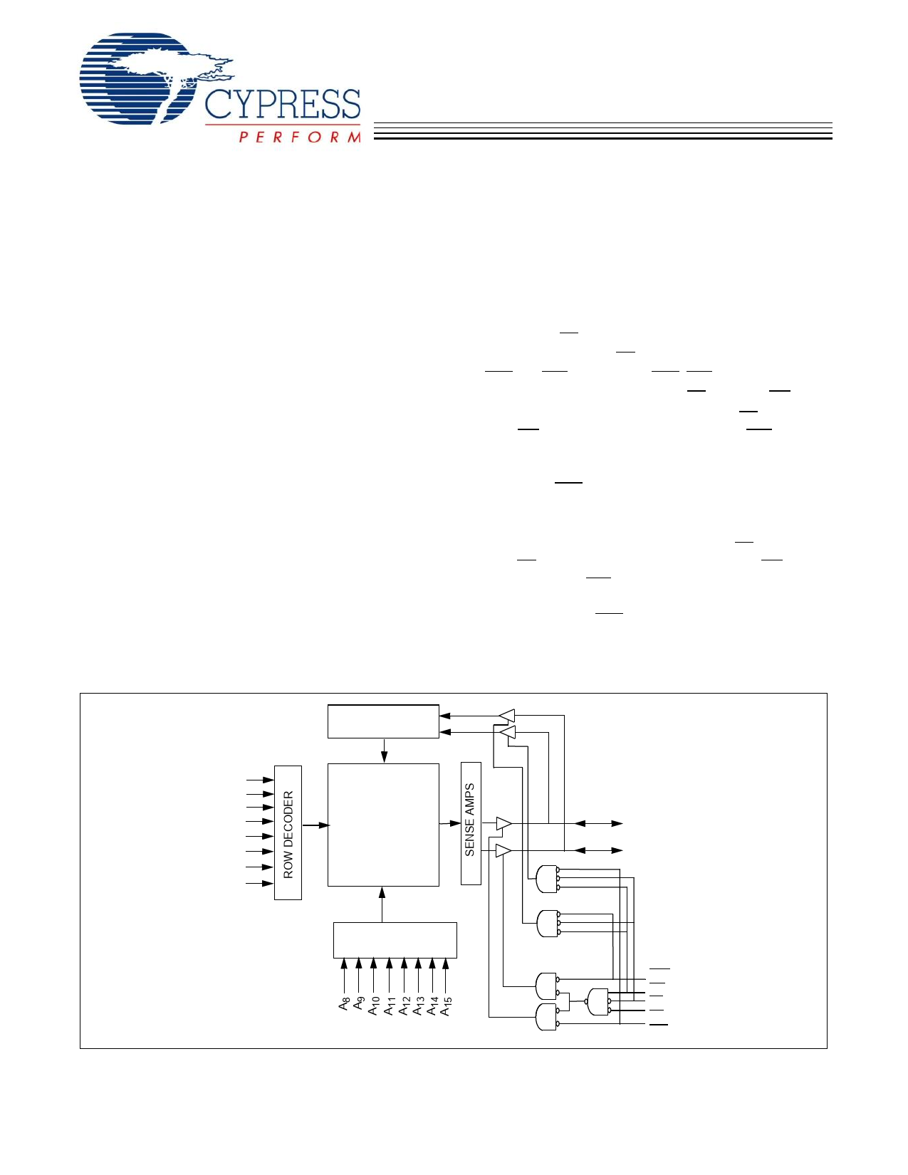
Logic Block Diagram
DATA IN DRIVERS
Functional Description
The CY7C1021D is a high performance CMOS static RAM
organized as 65,536 words by 16 bits. This device has an
automatic power down feature that significantly reduces power
consumption when deselected. The input and output pins (IO0
through IO15) are placed in a high impedance state when the
device is deselected (CE HIGH), outputs are disabled (OE
HIGH), BHE and BLE are disabled (BHE, BLE HIGH), or during
a write operation (CE LOW and WE LOW).
Write to the device by taking Chip Enable (CE) and Write Enable
(WE) inputs LOW. If Byte Low Enable (BLE) is LOW, then data
from I/O pins (IO0 through IO7), is written into the location
specified on the address pins (A0 through A15). If Byte High
Enable (BHE) is LOW, then data from I/O pins (IO8 through IO15)
is written into the location specified on the address pins (A0
through A15).
Read from the device by taking Chip Enable (CE) and Output
Enable (OE) LOW while forcing the Write Enable (WE) HIGH. If
Byte Low Enable (BLE) is LOW, then data from the memory
location specified by the address pins appears on IO0 to IO7. If
Byte High Enable (BHE) is LOW, then data from memory
appears on IO8 to IO15. See the Truth Table on page 8 for a
complete description of read and write modes.
For best practice recommendations, refer to the Cypress
application note AN1064, SRAM System Guidelines.
A7
A6
A5
A4
64K x 16
A3
RAM Array
A2
A1
A0
COLUMN DECODER
IO0–IO7
IO8–IO15
BHE
WE
CE
OE
BLE
Cypress Semiconductor Corporation • 198 Champion Court
Document #: 38-05462 Rev. *F
• San Jose, CA 95134-1709 • 408-943-2600
Revised August 14, 2009
[+] Feedback
Share Link: 