CY7C1021D(2009) データシートの表示(PDF) - Cypress Semiconductor
部品番号
コンポーネント説明
メーカー
CY7C1021D Datasheet PDF : 11 Pages
| |||
CY7C1021D
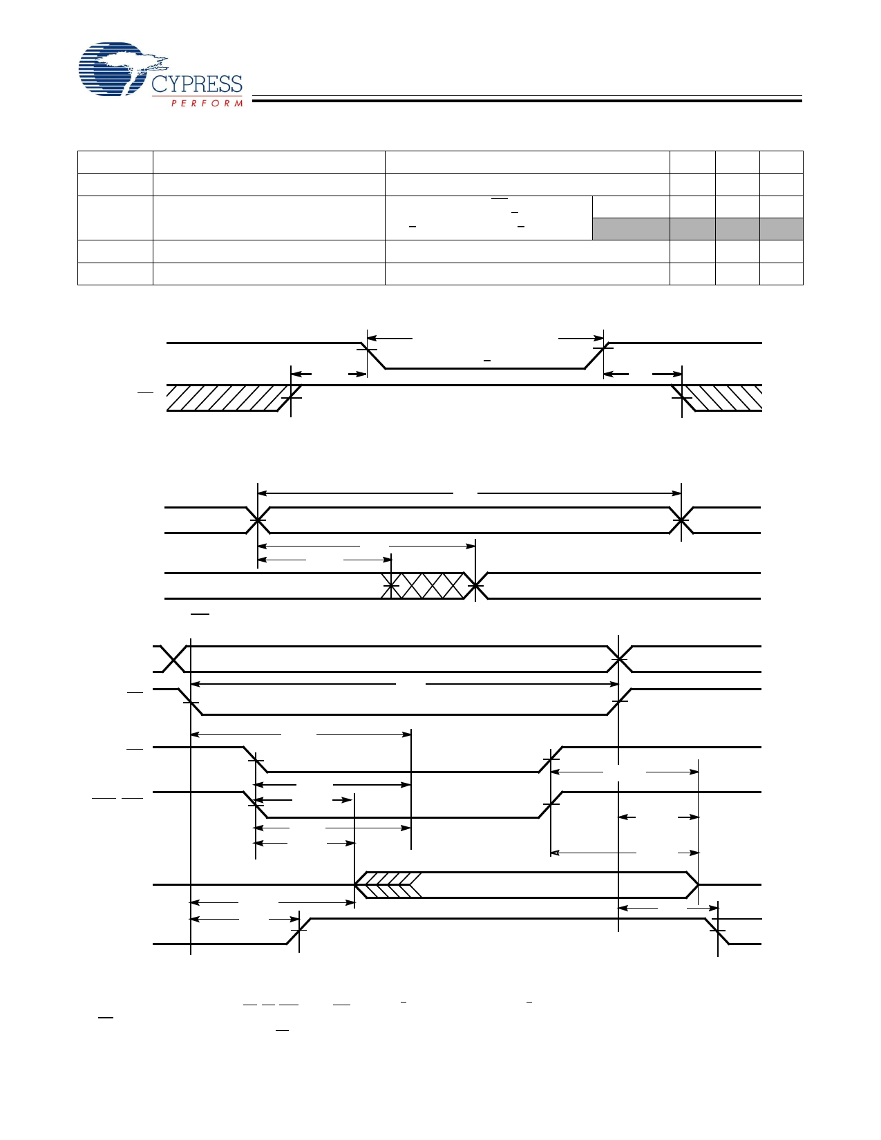
Data Retention Characteristics (Over the Operating Range)
Parameter
Description
Conditions
Min Max Unit
VDR
ICCDR
tCDR [3]
tR [12]
VCC for Data Retention
Data Retention Current
2.0
V
VCC = VDR = 2.0 V, CE > VCC – 0.3 V, Industrial
VIN > VCC – 0.3 V or VIN < 0.3 V
Automotive
3 mA
10 mA
Chip Deselect to Data Retention Time
0
ns
Operation Recovery Time
tRC
ns
Data Retention Waveform
DATA RETENTION MODE
VCC
4.5V
VDR > 2V
4.5V
tCDR
tR
CE
Switching Waveforms
Figure 3. Read Cycle No. 1 (Address Transition Controlled) [13, 14]
tRRCC
ADDRESS
DATA OUT
tAA
tOHA
PREVIOUS DATA VALID
DATA VALID
Figure 4. Read Cycle No. 2 (OE Controlled) [14, 15]
ADDRESS
tRC
CE
tACE
OE
BHE, BLE
tDOE
tLZOE
tDBE
tLZBE
DATA OUT
VCC
SUPPLY
CURRENT
HIGH IMPEDANCE
tLZCE
tPU
50%
DATA VALID
Notes
12. Full device operation requires linear VCC ramp from VDR to VCC(min) > 50 μs or stable at VCC(min) > 50 μs.
13. Device is continuously selected. OE, CE, BHE and/or BLE = VIL.
14. WE is HIGH for read cycle.
15. Address valid prior to or coincident with CE transition LOW.
tHZOE
tHZCE
tHZBE
HIGH
IMPEDANCE
tPD
ICC
50%
ISB
Document #: 38-05462 Rev. *F
Page 6 of 11
[+] Feedback
Share Link: 